Programmable Logic Puts MCU-based Designs on the Fast Track
The capabilities of large programmable logic devices such as field-programmable gate arrays (FPGAs) and complex programmable logic devices (CPLDs) have grown rapidly since they were first introduced decades ago as a replacement for glue logic and as an ASIC prototyping device. Embedded accelerators and microprocessors have made them strong candidates for many applications once considered the exclusive province of DSPs and ASSPs. Once designers understand the basics of FPGA and CPLD architectures, they can improve the performance, efficiency and design cycles of many designs.
Programmable logic had a long history of development before it reached its most advanced form in FPGAs and CPLDs. The difference in architecture between the two technologies is signaled by the names themselves. FPGAs are structured very much like a gate-array ASIC and were, in fact, originally used for prototyping ASICs. CPLDs are a network of programmable logic elements that are connected to create a much larger system.
Programmable Logic Basics
The basic configuration idea for FPGAs and CPLDs can be quickly understood by reviewing the characteristics of programmable array logic (PAL), which begins with a wide, programmable AND plane for ANDing inputs together. The OR plane is fixed, which limits the number of terms that can be ORed together. Basic logic devices, such as multiplexers, exclusive ORs, and latches are added and clocked elements such as flip-flops are also included.
This combination of circuit elements enables the designer to implement a large number of logic functions including clocked sequential logic needed for state machines. PALs are very fast devices that replaced much of the standard logic in previous-generation designs. Figure 1 shows a basic PAL in which the programmable elements (shown as fuses) connect both the true and complemented inputs to the AND gates. The AND gates, which are also known as product terms, are ORed together to form a sum-of-products logic array.
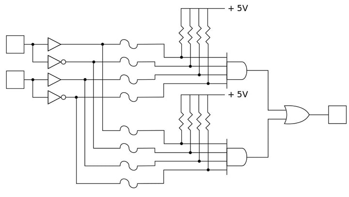
Figure 1: Simplified PAL
CPLDs and FPGAs create a happy and very extensible medium between PALs and ASIC gate arrays. CPLDs are as fast as PALs but are more complex. FPGAs approach the complexity of gate arrays and are programmable.
CPLD Architectures
Although every CPLD vendor has its unique implementation, all CPLDs have the common characteristic of consisting of function blocks (FB), input/output blocks (I/O), and an interconnect matrix. CPLDs are programmed using elements specific to the technology of the manufacturer. The memory device can be EPROM cells, EEPROM cells, or Flash EPROM cells. Figure 2 shows the architecture of a typical CPLD.

Figure 2: Simplified CPLD architecture
FPGA Architectures
FPGA architectures are similar to ASICs and quite different from CPLDs. A generic FPGA architecture consists of an array of configurable logic blocks (CLBs), I/O pads, and programmable interconnect as shown in Figure 3. Clock circuits are added to drive clocks signals to each logic block. Arithmetic logic units, memory, and decoders are also typical elements.
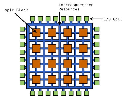
Figure 3: Basic FPGA architecture
FPGA logic is contained in CLBs, which contains the RAM used to create combinatorial logic functions, which are also known as lookup tables (LUTs). It also contains flip-flops for clocked storage elements, and multiplexers for routing the logic within the block and between external resources. Multiplexers are also used for polarity selection and reset and clear input selection.
Configurable I/O blocks consist of an input and output buffer with three state and open collector output controls. The polarity of the output can usually be programmed for active high or active low output and often the slew rate of the output can be programmed for fast or slow rise and fall times. Flip-flops are usually included on the inputs and outputs. Flip-flops are used on the inputs so that there is not much delay on a signal before reaching a flip-flop, which would increase the device hold time requirement. On the outputs, flip flops allows clocked signals to be output directly to the pins without encountering significant delay.
Avoiding the consequences of signal delay creates an interconnect hierarchy in which long lines connect critical CLBs that are physically far from each other on the chip. (They can also be used as buses.) Short lines connect individual CLBs located close to each other. Switch matrices, similar to those in a CPLD, connect long and short lines in specific ways. Programmable switches inside the chip allow the connection of CLBs to interconnect lines and interconnect lines to each other and to the switch matrix.
Buses are created using three-state buffers that join CLBs to a long line. Clocks are distributed through the FPGA primarily through long lines called global clock lines, specifically designed for low impedance and fast propagation. These are connected to the clock buffers and to each clocked element in each CLB.
FPGA Implementation Technologies
FPGAs are traditionally described according to the memory technology used to store the logic configuration for the FPGA. Four are in use today, each with its advantages and disadvantages: SRAM-based FPGAs, SRAM with internal Flash memory, Flash-based, and antifuse (also known OTP because they are one-time programmable).
- SRAM-based FPGAs store logic cell configurations in static memory organized as an array of latches. Because SRAM is volatile, this type of FPGA must be programmed each time the system boots. There are two basic modes of programming:
- Master mode, which is when the FPGA reads configuration data from an external source, such as an external Flash memory chip.
- Slave mode, in which the FPGA is configured by an external master device, such as a processor. Typically, this is done with either a dedicated configuration interface or by using a boundary-scan (JTAG) interface.
- SRAM-based FPGAs with an internal Flash memorycontain internal flash memory blocks that eliminate the need for external non-volatile memory.
- True Flash-based FPGAs use Flash as a primaryresource for configuration storage and therefore does not require an external non-volatile memory. This technology is less power consumptive than SRAM-based FPGAs and is more tolerant to the effects of radiation.
- Antifuse-based (OTP) FPGAs are different from the previously mentioned technologies because they can be programmed only once. (An antifusedevice does not conduct current initially, but can be burned into a conductive state.)
Modern SRAM-based FPGAs have the highest densities, but consume a lot of power and need an external non-volatile memory to store configurationbitstream. SRAM-based FPGAs with an internal flash module do not need an external configuration memory. Flash-based and antifuse-based FPGAs consume much less power than their SRAM-based counterparts.
Processor Cores
Although programmable devices were first developed as glue logic replacements, as gate density grew, FPGA and CPLD vendors began to add circuits with dedicated functionality to complement their unassigned gates and logic functions. The result is called a system on a programmable chip (SoPC), in which entire systems consisting of complicated devices such as processors are integrated into a single programmable logic device.
Today, most FPGA and CPLD vendors offer product families that provide the functionality of MCUs and other IP cores. Using cores give system designers access to familiar development tool sets, operating systems, and selectable performance to fit the application.
There are two kinds of cores hard and soft. Soft-cores are described by logic function not physical implementation and typically consist of HDL code. Hard cores, as the name implies, have physical implementations. When used with FPGAs and CPLDs, hard cores are usually called embedded cores because they are embedded in the die and surrounded by programmable logic.
Soft cores have two implementation options. The first and more common is to use one that the vendor already supports (it is still up to the design team to add I/O and other peripherals). Alternatively, the design team has the option of purchasing the HDL code and incorporating it into the HDL code for the FPGA.
To speed development time and generally make it easier for system designers, programmable logic vendors offer a variety of popular MCU cores. Altera, for example, makes available cores from ARM, Freescale Semiconductor, and Intel as well as its own Nios® and Nios II processor cores that do not require royalty payments.
Cypress Semiconductor's PSoC® 5 integrates configurable analog and digital peripheral functions, memory and a microcontroller. The PSoC 5 uses the 67 MHz ARM® CortexTM-M3 core. The PSoC 4 integrates the ARM Cortex-MO core and the PSoC 3 integrates Intel's 8-bit 8051 MCU core.
SoPC Advantages
There are several compelling reasons to consider using SoPCs that include MCU functionality. The first is to recognize the hidden costs of using a dedicated MCU. If the part does not have the right mix of features, for example, external logic and software must be developed to fill the functionality hole. While MCU vendors offer devices with specialized features to suit specific applications, these chips do not take into account dynamic market conditions that may require, for example, a new interface or peripheral on very short notice.
Designing a new microcontroller in current state-of-the-art process technologies is very expensive and has a long lead time. MCU vendors have responded by adding more features some of which cannot be used in a particular application. This increases product cost, which can be critical in cost-sensitive markets.
SoPC implementations neatly address these problems. The chip can be programmed and reprogrammed as needed during the design process, enabling more rapid prototyping and fast time-to-market. SoPCs also can be upgraded in the field if requirements change even after the devices are deployed in a product.
Development risk is minimized because of the opportunity for comprehensive verification, firmware development, and field testing. Design engineers can run the SoPC in-system to exercise the device real-world situations to identify potential design flaws.
Developing system-level software on a single SoPC can radically shorten the overall software development cycle. Using the FPGA vendor's tools make it easier to find bugs and identify compatibility issues. If the desired functionality cannot be implemented in the software, the requirements for additional hardware support can be recognized sooner rather than later. For previously undiscovered flaws or to add new features, SoPCs can be modified quickly without large nonrecurring engineering costs or long manufacturing cycles. They also have demonstration models available for salespeople to use to increase the probability of securing a customer pre-order. In addition to their advantages for prototyping, in many instances SoPCs can also be used for volume production.
Example: Processor Flexibility for Automobile Electronics
Automobiles have unlimited appetite for integrated MCUs. Every major system engine control, braking, chassis and entertainment, to name just three has at least one. Traditionally, the demand was met with application-specific MCUs, but as the number of applications (and MCU variants) increases, this strategy is being questioned. Automakers are looking for more flexible, easily customized solutions and in some instances FPGAs are the answer.
FPGAs implementing graphics controllers have already gained acceptance in automotive electronics in part because as the computational and I/O requirements grow, FPGAs can quickly be reconfigured to meet the new challenges without large non-recurring engineering costs. Figure 4 shows how Altera's Cyclone® IV can be reconfigured to handle increasingly demanding applications.
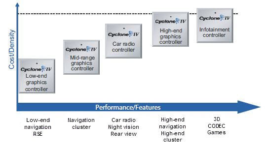
Figure 4: Altera's Cyclone IV is a cost effective solution for a range of automotive graphics applications.
In every implementation, Altera's Nios II MCU core can be generated automatically according to the designer's specifications. The can be parameterized using Altera's SOPC Builder, found in the Quartus® II design software, and can be implemented with the exact functionality and corresponding consumption of logic required.
Nios II uses RISC architecture with separate 32-bit address and data buses. Both buses have their own caches. The designer makes the final decision, however, about whether separate caches are used for code and data or, have both in shared memory. Although Nios II has the functionality of other advanced processors, settings determine their character. For instance, the hardware multiplier, the barrel shifter, and the hardware divider can be selected as options. The same is true for the instruction and data cache, which can be varied in size or completely excluded.
Conclusion
The flexible solutions available through the use of SoPCs give designers the opportunity to develop the exact microcontroller needed for a specific application. The chip can be programmed and reprogrammed as needed during the design process, enabling rapid prototyping and fast time-to-market. Field testing can be done immediately after design process or even in parallel. SoPCs can also be upgraded in the field if requirements change even after the devices are deployed in a product.