Image Processing in FPGAs for Industrial Applications

Image Source: Author
By Adam Taylor for Mouser Electronics
Published February 28, 2023
Introduction
Field-programmable gate arrays (FPGAs) are excellent for implementing image processing systems. Their highly parallel logic architecture enables the implementation of high-resolution, high-frame-rate image processing algorithms, making FPGAs ideal for many applications, ranging from autonomous driving to robotics. Often, image processing solutions are implemented within a heterogeneous system-on-chip (SoC), which combines programmable logic with hard Arm® processor cores. However, depending on the application, these processors may not be fully utilized, relegated to preliminary IP core configuration following power up. In this case, it is often best to use a traditional FPGA, with either configuration state machines for the IP cores or using a soft processor core.
In this project, we will create an image processing pipeline on an AMD Artix™ 7 FPGA using the AMD AC701 evaluation board. This board will use the FMC interconnect to connect to a MIPI camera, with the output video displayed over HDMI.
The bill of materials for the project consists of the following:
- AMD AC701 evaluation board
- Digilent FMC PCAM adapter
- Digilent Pcam 5C fixed-focus color camera module
- HDMI display
- HDMI cables
We will use the following software to develop this application:
- Vivado™ 2022.1
- Vitis™ 2022.1 (How to install Vitis, step-by-step instructions)
- Matlab & Simulink – R2021b
Basic Hardware Design
First, we need to create a system that can implement a standard image passthrough. This will configure the camera and the IP blocks correctly within the FPGA to receive an image and pass it though the processing chain via HDMI. Because these devices are very versatile, we can configure them for the desired output format. Both the Pcam 5C camera module and the HDMI chip are configured over the same I²C link.
To configure the camera, HDMI chip, and internal IP cores, we need to implement an AMD MicroBlaze™ soft processor core. More information on mastering MicroBlaze can be found here.
The following are the IP blocks required for the transparent passthrough:
- MicroBlaze, configured to provide both AXI interfaces for instruction and data
- MicroBlaze Debug Module
- AMD AXI Interrupt Controller, connected to the MicroBlaze interrupt port
- AXI IIC, connected to the external I²C bus for the camera and HDMI configuration, as well as to the AXI Interrupt Controller to enable an interrupt-driven approach
- AMD MIPI CSI2 RX Subsystem, received the MIPI streams from the camera when configured
- AMD LogiCORE™ IP Sensor Demosaic core, which converts the raw images from the camera to a RGB pixel representation
- Video Frame Buffer Write, which stores image frames in the DDR3 memory
- Video Frame Buffer Read, which reads image frames from the DDR3 memory
- Video Timing Controller, which generates the timing waveforms for the desired output timing (in this case 1080p at 60 FPs)
- Video Processing Subsystem, which performs color space conversion from RGB to YUV
- AXI Stream to Video Out, which converts the AXI Stream internal video to parallel video with appropriate syncs for the HDMI chip
- Clocking wizard, used to generate the clocks internal for the FPGA (These are 200MHz for the MIPI and MIG reference clocks and 150 MHz for the video pipeline. Internally the MicroBlaze runs off the slower MIG generated clock.)
- UART Lite for communication of processing with the user.
These modules are connected using both AXI Stream and AXI4 interfaces. The final block design can be recreated by using the block diagram script in the AMD Vivado™ ML Edition Tcl window as shown in Figure 1.
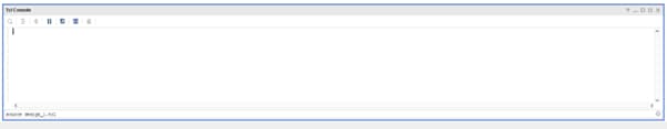
Figure 1: Tcl command window. (Source: Author)
This will start rebuilding the project in Vivado, as shown in Figure 2. This process might take a few minutes to complete.
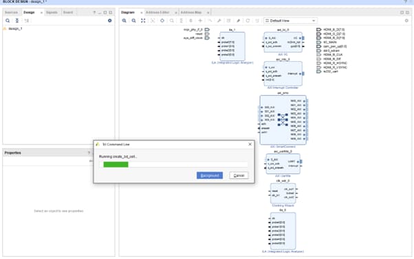
Figure 2: Recreating the project. (Source: Author)
Once the process is complete, you can explore the design (Figure 3).

Figure 3: The completed design. (Source: Author)
Create a new top-level HDL wrapper, as shown in Figure 4.
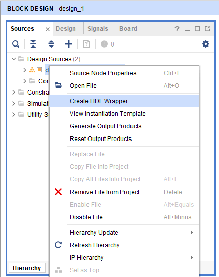
Figure 4: Creating the HDL wrapper. (Source: Author)
Add the XDC constraints, which define the pins. Select “Add Sources” and select constraints (Figure 5).
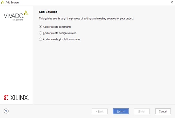
Figure 5: Adding the constraints. (Source: Author)
Select the IO.xdc file (Figure 6).
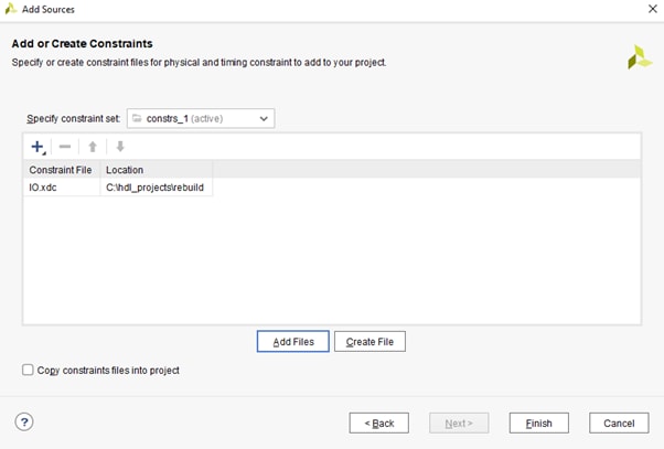
Figure 6: Selecting the IO.xdc file as a constraint. (Source: Author)
We can now build the project and generate the bitstream. Once the bitstream is available, you can export it as an Xilinx Support Archive (XSA) file to enable the software to be developed in Vitis (Figure 7).
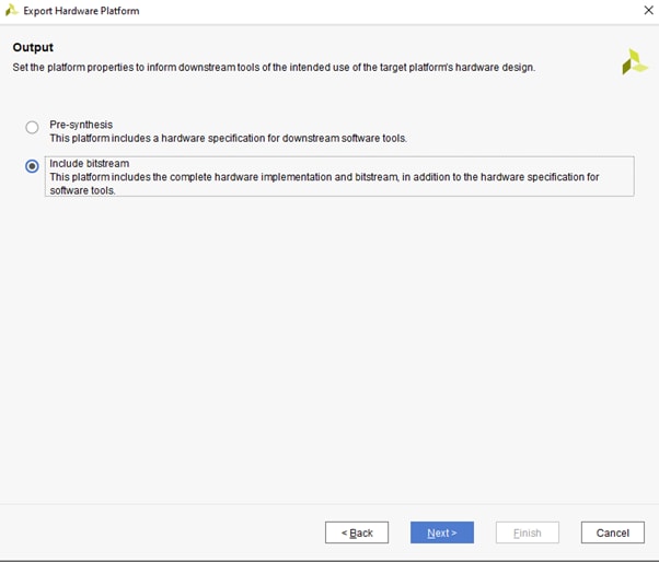
Figure 7: Exporting the hardware to Vitis. (Source: Author)
Open Vitis and select a working directory for the workspace (Figure 8). This is where all the files and applications will be stored.
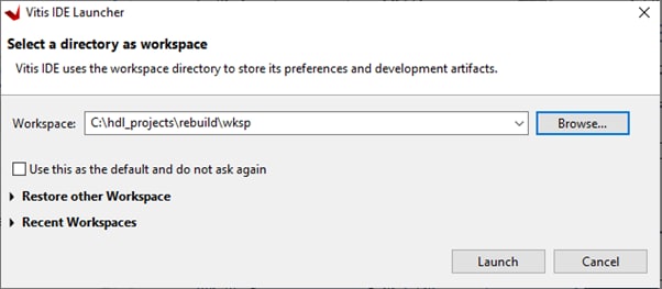
Figure 8: Selecting the workspace. (Source: Author)
In Vitis, create a new application project, target the just exported XSA, and select the “Hello World” application (Figures 9 – 13).

Figure 9: Selecting the application project. (Source: Author)
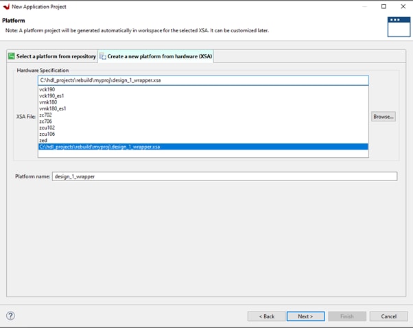
Figure 10: Selecting the exported XSA file. (Source: Author)
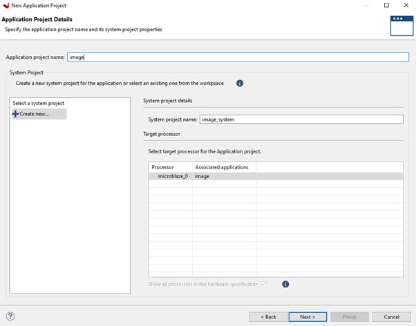
Figure 11: Selecting the target processor. (Source: Author)
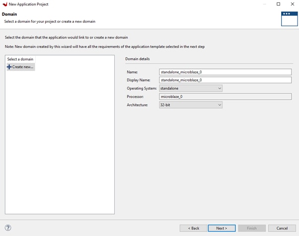
Figure 12: Selecting the domain. (Source: Author)
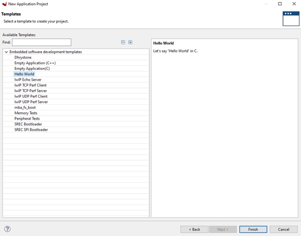
Figure 13: Selecting the "Hello World" application. (Source: Author)
Replace the files in the src folder in the workspace created in Figure 8 with those shown in Figure 14.

Figure 14: Copying the files to the workspace. (Source: Author)
These files will then appear under the project source (Figure 15).
Figure 15: Ensuring that the files were imported. (Source: Author)
Build the application (Figure 16).
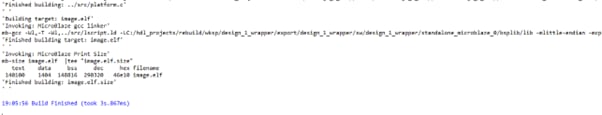
Figure 16: Building the application. (Source: Author)
Create a debug application to download to the AC701 evaluation board via JTAG. Assemble the FMC Pcam adapter and Pcam module on the board (Figures 17 – 19).

Figure 17: Setting up the hardware. (Source: Author)
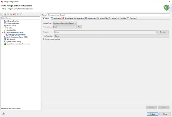
Figure 18: Configuring the debug application. (Source: Author)
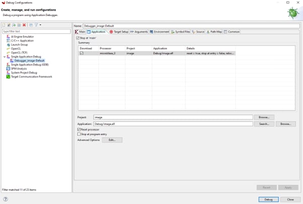
Figure 19: Viewing debug application settings. (Source: Author)
This will download and run on the target showing and passthrough image when connected to an HDMI target. If you want to explore the software design, look at the software applications in the AMD Vitis™ unified software platform. Note that there are several I²C switches that must to be configured to enable communication with the camera and the HDMI chip (Figure 20).

Figure 20: Simple RGB image passthrough (Source: Author)
To create the IP core that performs the edge detection, we will use Matlab and Simulink to create the IP block which can be dropped into the image processing chain.
Edge Detection Algorithm
Within Matlab, create a new Simulink diagram and add in the following elements:
- From Multimedia File, this will allow the use of an AVI file or MPEG from test benching
- From Frame to Pixels, this will convert the output video into a pixel stream
- From Pixels to Frame, this will convert a pixel stream to a frame
- Two Video Viewers
Create a submodule and add the following:
- Sobel Filter, the output of this is a 1 or 0 depending on the presence of an edge
- Constant blocjs set to 0 and 255
- Switch
- Pixel Streamer Aligner
- Create another submodule
Image merging submodule
- Two gain blocks: one set for 1-Alpha and the other for alpha
- Delay element
- Sum
The diagrams should look like Figures 21 – 23.
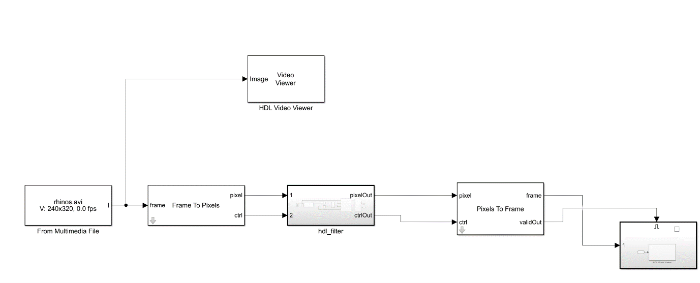
Figure 21: High-level design. (Source: Author)

Figure 22: HDL filter block. (Source: Author)
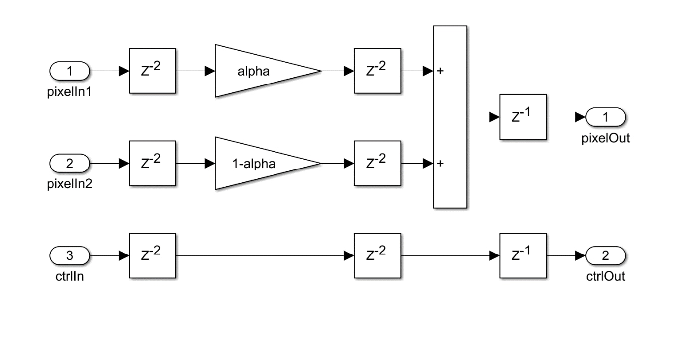
Figure 23: Image overlay. (Source: Author)
With these modules, we can run a simulation and compare the results of the input image to the output image.
In the output video, notice how the edges are enhanced as the results of the Sobel are superimposed on the input video (Figure 24).
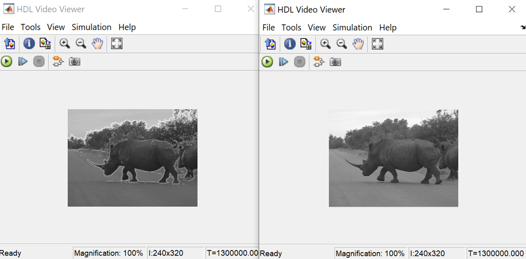
Figure 23: Simulation in Simulink. (Source: Author)
To generate the HDL, we can use the HDL Workflow assistant with the SoC Blockset to generate an IP module that has AXI Stream Interfaces and AXI4 Lite configuration registers.
The key element of the IP creation is mapping the pixel stream and control ports to the AXI Stream interfaces on the resultant IP block. This makes it very easy to integrate the IP block within our Vivado design (Figures 25 and 26).
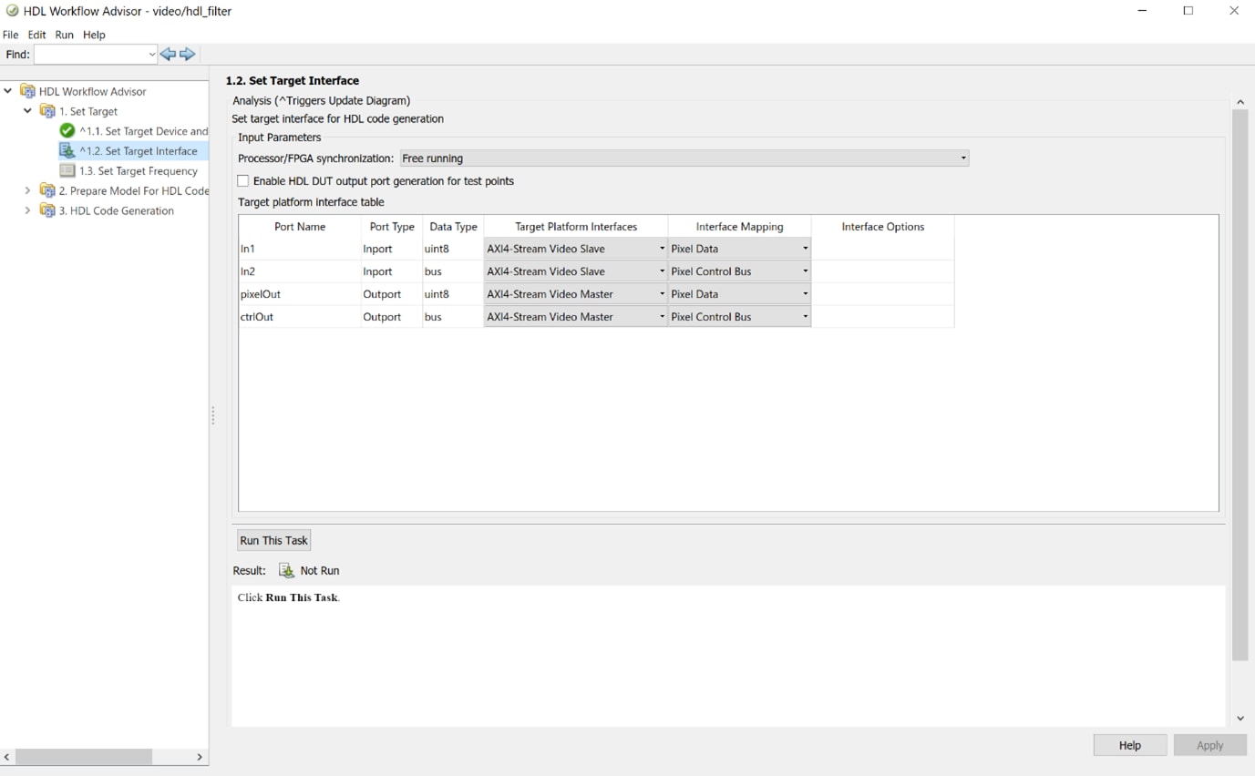
Figure 25: Selecting the AXI interface. (Source: Author)
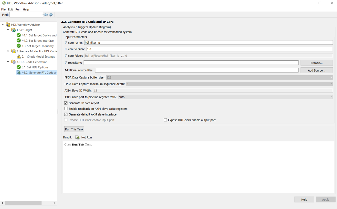
Figure 26: Generating the HDL. (Source: Author)
Once generated, we can add this IP core back in the Vivado project to make a new IP repository and add in the IP we just created (Figure 27).
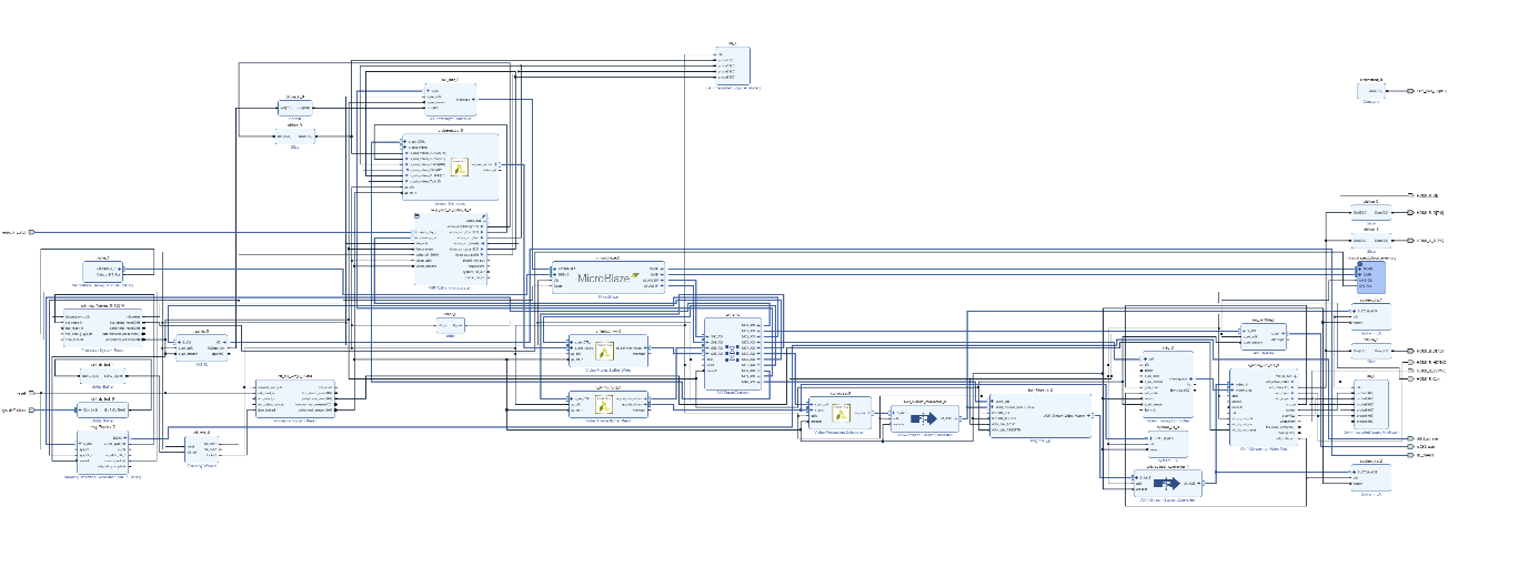
Figure 27: Updated Vivado diagram. (Source: Author)
Add the IP block into the Vivado design, as it is going to be working in grayscale. We can add it between the VPSS and the AXIS-to-Video Out block. This makes sense, as the Y channel of the YUV444 output from the VPSS is the luminance channel. Add in a AXI subset convertor between the blocks and take only the lower 8 bits of the TData stream, as that is where the information we want is stored. On the output of the IP block, add another AXIS Subset convertor (which converts pads the 8-bit TData to 24 bits), setting the UV elements to 0x80 and the Y element to the output of the IP block.
This design can then be rebuilt and the bitstream generated. Once the bitstream is available, you can export the XSA file and update the XSA file in Vitis. This will provide a new bit file for the FPGA design, which includes the IP block. By default, you don’t need to change or enable anything in the software, so the application should start running immediately. Note that the output on the HDMI display shows a grayscale image(Figure 28).
Figure 28: The resulting output image. (Source: Author)
Wrap Up
This project has shown that an image processing system can be easily created targeting an AMD FPGA.
AMD, the AMD Arrow logo, Artix, MicroBlaze, LogiCORE, Vivado, and Vitis, and combinations thereof are trademarks of Advanced Micro Devices, Inc. Other product names used herein are for identification purposes and may be trademarks of their respective owners.