Resistive and Capacitive Touch Technology: How Does It Work?
The booming Touch Sensing market is fueled in part by continued innovation, and has created a diverse range of touch technologies including resistive touchscreens implemented in many cost-effective designs, projected mutual capacitive methods used in smartphones, and optical and piezoelectric based devices used in creating very large scale touch displays. But how do they work and why are they used? Discussed here are two of the most common touch technologies: resistive touch sensing and capacitive touch sensing.
Resistive Touchscreens
Why are they used?
Although the capacitive touch market can claim the highest growth rates, resistive touchscreens are widely available and remain in common use. Resistive touch technology is relatively simple, and can enable higher resolution at a lower cost when compared with capacitive touchscreens.
Resistive touch sensing is different from other touch methods in that the sensor is mechanically actuated. That is to say, there are two conductive layers separated by an air gap, and a pressing force is required to bend the top layer into contact with the bottom. This can be a problem or benefit, depending on the application. The touch sensor is easy to interface and can be activated with a broad range of objects such as a stylus, pencil eraser, fingernail, or even a gloved finger.
However, the need for a flexible top layer means that the screen is subject to mechanical wear, and although not affected by dust or water, it is more susceptible to scratches and damage from sharp objects. Typical resistive touchscreens also rate the poorest in optical quality, transmitting only about 80% of light from the display below it. Yet the affordability, simplicity, and versatility of resistive touchscreens often make the technology an attractive option for many designs.
How do they work?
The two conductive layers of a resistive touchscreen must be transparent, and so they are usually composed of indium tin oxide (ITO) . The bottom layer is deposited on glass substrate and is separated from the top ITO layer by transparent spacer dots. The surface of the screen is coated with a flexible layer of protective insulation which will often feature scratch resistance and anti-glare properties.
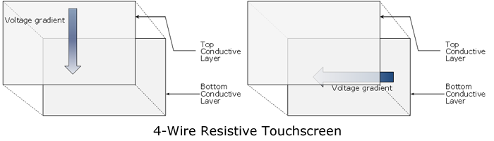
There are several methods for determining touch location from a resistive screen. The simplest uses only four wires: two connected to the left and right sides of the bottom conductor, and two connected to the top and bottom of the other conductor. A voltage gradient is applied across one of the uniformly resistive ITO layers (e.g. the bottom layer) and when contact is made with the top layer the resulting circuit resembles a voltage divider. The voltage is probed at the top layer to determine the x-coordinate of the touch location. This process is repeated for the y-axis by applying a potential across the top conductor and measuring the bottom layer voltage.
Resistive 4-wire touchscreens and corresponding controllers are ubiquitous and low cost. However, because this technology uses the flexible layer for measurement, wear and tear on the top ITO sheet can change the resistance characteristics of the conductor, resulting in a potentially significant decline in accuracy. For larger screens, this drawback as well as sensor drift become more apparent. The 4-wire method is therefore most preferable for smaller touchscreens.
The 5-wire resistive touchscreen is an attempt to resolve the issue of using a flexible upper layer for measurements. This technology implements both the "left-right" and "top-bottom" wires of the 4-wire scheme as electrodes attached instead to the four corners of the stable bottom layer, with the fifth wire functioning only as a top layer voltage probe. The bottom layer is therefore used for both X and Y-axis measurements, increasing the overall durability and accuracy of the touchscreen.
 Surface Capacitive Touchscreens
In comparison, capacitive touch technology can offer superior optical qualities. Also, a flexible layer is not required, so capacitive screens can be made highly durable and environmentally resistant. Surface capacitive touch technology differs from projected capacitive technology in that the substrate is coated with only a single, uniform conductive layer. The conductor is protected by additional layers of insulative material, but thickness is limited due to trade-off with touch sensitivity. There are many different sensing methods used in the industry but all are based on the principle of measuring the resulting increase in capacitance when a finger or conductive stylus is brought near the conductive layer.
Capacitive sensing buttons and sliders may not need to be transparent, so a potentially broad selection of materials can be used for the conductive layer (e.g. typical PCB copper). Also, a wide variety of sensing techniques are possible. For example, changes in capacitance can be detected by applying a time-varying voltage to the conductive layer and measuring the change in RC behavior of the circuit. Charge transfer methods are another option; the increased sensor capacitance from a finger touch results in a greater transfer of electrical charge to a reference capacitor, which is measured as the potential across it. While touch buttons are made from a single conductive pad, sliders are usually implemented as a series arrangement of multiple pads.
Surface capacitive designs for a touchscreen are a bit more constrained. ITO or similar transparent conducting oxides are chosen for the conductive layer because sensor transparency is a common requirement. Electrodes are precisely arranged around the conductive layer to generate a uniform AC voltage throughout the sheet. When a finger or conductive stylus is placed at a point on the screen, the user becomes a capacitively coupled path to ground. The resulting current draw is then measured, typically, from each corner of the conductive sheet and the values are used to calculate the xy-coordinates of the touch location.
While surface capacitive designs offer better optical transmission than resistive screens and are not burdened by the greater complexity of projected capacitive screens, they can suffer from parasitic capacitive coupling and have, in general, the poorest resolution of the three. Surface capacitive touchscreens are well suited for applications such as kiosks and basic industrial controls.
Projected Capacitive Touchscreens
Most projected capacitance touchscreen sensors consist of two transparent conductive layers, typically of ITO, separated by a thin insulator to form a grid pattern. Some of the newest and thinnest designs implement this in a single layer by sputtering the ITO grid on a single substrate.
In the smartphone industry, projected capacitive touchscreens are becoming increasingly more common due to a variety of advantages over other touch technologies such as long product life, high durability, superior optical qualities, and true multi-touch sensing. The projected capacitive screen of a typical smartphone may have a couple hundred electrode intersections; however a much higher resolution can be achieved with special algorithms that interpolate the values of adjacent electrodes.
Projected capacitive touch technology can be further classified into either self-capacitive or mutual capacitive screens.
Self-Capacitive Screens
Self-capacitive screens sense touch by measuring the sum of parasitic (self-) capacitance and the capacitance added by a finger or conductive stylus. In terms of sophistication, this method is somewhere between resistive touchscreens and the more complex mutual capacitive type screens.

Electrodes are laid out in a 2-layer grid and measurements are taken not from an electrode intersection, but from a row and column electrode pair. This presents a problem for multi-touch functionality. When the screen is touched at two different locations, there are two sets of possible points that can be interpreted by the touch device (this forms a rectangle, with each pair on a diagonal), with no way for software to resolve which pair corresponds to the actual locations touched. The two false locations are called "ghost points". Fortunately, many multi-touch gestures (such as a "pinch") are insensitive to this effect.
Although many newer designs, especially for smartphones, have moved toward mutual capacitive touchscreens, self-capacitive technology is still in use and continues to improve.
Mutual Capacitance Screens
Mutual projected capacitive sensors are a newer technology, and measure the capacitance between electrodes (instead of electrode-to-ground). So, unlike self-capacitive touchscreens, measurements can be taken at each electrode intersection. The intersections are "scanned" individually, typically by driving a column-electrode and then quickly scanning every row-electrode that intersects it. This is advantageous because it means that the hardware structure supports unambiguous sensing of virtually unlimited simultaneous touches.
Mutual capacitance also allows for a greater range of sensor pattern designs, which can help maximize the signal-to-noise ratio (SNR). This is fortunate because measured capacitances can be in the femtofarad range, making LCD noise especially problematic. Still, mutual capacitive technology is gradually replacing its self-capacitance counterpart in many applications, being generally more robust and less optically obstructive.
Looking Forward
These are certainly not the only touch technologies in use today. Many others exist, each with their specific advantages. However, technology and innovation continue marching onward; capacitive touchscreens are being developed that work even while wearing gloves and the world may soon see projected capacitive displays with hover sensing functionality. Meanwhile, Mouser Electronics continues to be a leader in offering the latest products and tools for pressing ahead in this growing industry.