The Ultimate Guide to Silicon MOSFET Technology
Types, Parameters, and Design Applications
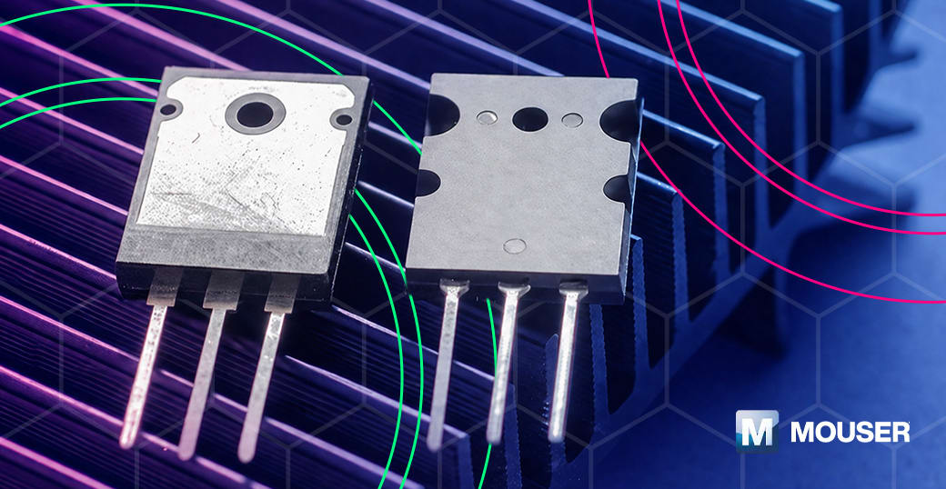
Image Source: Mouser
By Simon Duggleby, Mouser
Published November 20, 2026
If there is one silicon device that almost everyone has used, it’s a MOSFET. MOSFET technology underpins applications ranging from integrated digital processors to discrete power switches and analogue amplifiers. This guide focuses primarily on discrete silicon MOSFETs used in power and analogue circuits.
What Does MOSFET Stand For?
A MOSFET is an acronym for a metal-oxide-semiconductor field-effect transistor.
MOSFETs are versatile components that come in a variety of sizes, packages, and designs. But which silicon MOSFET is best for a specific application or project? And will silicon MOSFETs remain the most popular choice for years to come?
What Is a Silicon MOSFET?
A silicon MOSFET is a semiconductor device commonly used as an electronic switch or as a power-control element. Its name comes from its structure, which consists of a metal gate separated from a semiconductor channel by a thin insulating oxide layer. Unlike bipolar junction transistors (BJTs), which require continuous base current during conduction, MOSFETs are voltage-controlled devices that can operate as switches or amplifying elements. This insulated-gate structure gives the device a very high input impedance, allowing it to control large currents while requiring very little drive power.
For a quick breakdown of common circuit design queries and troubleshooting tips, refer to MOSFET FAQs.
Silicon MOSFET Structure and Physical Construction
The structural architecture of a discrete silicon MOSFET (Figure 1) dictates its electrical performance, power-handling limits, and suitability for specific applications. A MOSFET is fundamentally a four-terminal device with gate, drain, source, and body terminals. In most discrete power MOSFETs, the body is internally connected to the source, leaving three externally accessible terminals:
- Gate (G): The control terminal, consisting of a metal or heavily doped polycrystalline silicon layer that is physically and electrically isolated from the substrate.
- Drain (D): One end of the channel conduction path, conventionally treated as the current-entry terminal for an N-channel MOSFET.
- Source (S): The terminal used as the reference for gate-to-source voltage and the opposite end of the channel conduction path.
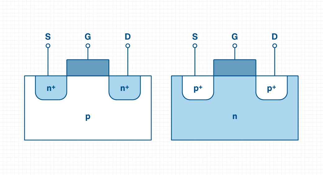
Figure 1: A structural diagram of an N-Channel MOSFET Vs a P-Channel MOSFET. (Source: Mouser)
The defining element of this device structure is the gate insulator, a microscopically thin layer of silicon dioxide (SiO2) grown directly over the silicon substrate. This barrier provides very high DC isolation, requiring almost no steady-state gate current. The discrete power MOSFET structure also creates an intrinsic body diode with a fixed orientation between source and drain. This diode conducts when forward-biased, whereas the enhanced MOSFET channel can conduct current in either direction. The body (or substrate) is the underlying silicon material in which the MOSFET structure is created.
How a Silicon MOSFET Works
MOSFET operation is controlled by the voltage applied between the gate and source terminals (VGS). When the VGS reaches the threshold voltage (VGS(th)), a conductive channel forms. The threshold value represents the onset of conduction at a small specified current, not full enhancement. Switching applications require the gate voltage specified for the desired on-state resistance (RDS(on)) and drain current.
MOSFETs are available in two channel types:
- N-type (NMOS) devices, which use electrons as the primary charge carriers. Because electrons move more easily through silicon than through holes, NMOS devices typically offer lower RDS(on), higher current capability, and better switching performance. As a result, they are the preferred choice for most power-switching applications.
- P-type (PMOS) devices use holes as the primary charge carriers. Their lower carrier mobility generally results in higher RDS(on) than comparable NMOS devices. However, PMOS devices remain useful in applications requiring simple high-side switching, where they can be driven directly without specialised gate-drive circuitry.
Silicon MOSFET Types
Silicon MOSFETs are classified by three main criteria: enhancement-mode vs depletion-mode operation, N-channel vs P-channel, and vertical vs. lateral structure.
Enhancement Mode vs. Depletion Mode MOSFETs
The primary distinction between MOSFET operating modes is whether the device is normally on or normally off. Enhancement-mode devices are normally off and require a gate-to-source voltage of the appropriate polarity and magnitude to create a conductive channel. By contrast, depletion-mode devices are normally on. Depletion-mode devices are uncommon, but remain important in specialised applications, such as current sources.
NMOS vs. PMOS: N-Channel and P-Channel MOSFETs
As mentioned, NMOS devices use electrons as their charge carriers, while PMOS devices use holes. Because electrons have higher mobility in silicon, NMOS devices achieve a lower on-resistance and higher current capability. This makes NMOS the preferred choice for most power-switching applications. PMOS devices, however, remain valuable in high-side switching circuits, where they can often be driven more simply than an equivalent NMOS. Therefore, designers frequently use NMOS devices where efficiency is critical and PMOS devices where circuit simplicity is the priority.
Lateral vs. Vertical Structure
While the preceding classifications focused on electrical behaviour, the lateral or vertical structure of a MOSFET describes its physical implementation. This structure affects the voltage rating, current capability, on-resistance, and suitability for specific applications.
Lateral MOSFETs (Figure 2) conduct across the silicon surface, resulting in smaller gate-to-drain and gate-to-source capacitances. However, they typically handle less voltage and current than vertical MOSFETs, making them best suited to integrated circuits, radio frequency (RF) amplifiers, and lower-power applications.
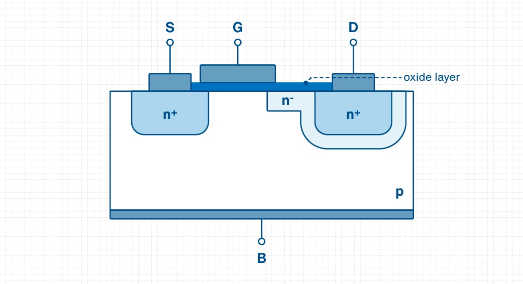
Figure 2: A structural diagram of a lateral silicon MOSFET. (Source: Mouser)
In contrast, vertical MOSFETs (Figure 3) conduct current through the thickness of the silicon die from a top source to a bottom drain. Because lateral layouts are unsuitable for high-voltage applications, nearly all discrete power MOSFETs used in power supplies, motor drives, and inverters employ a vertical structure, allowing much larger current-carrying areas and higher voltage ratings. Modern vertical power MOSFETs are further optimised with trench gate technology, which embeds the gate vertically into the silicon substrate to maximise channel density and minimise RDS(on), and superjunction structures, which use alternating vertical N-type and P-type columns to achieve low resistance while maintaining high breakdown voltage.
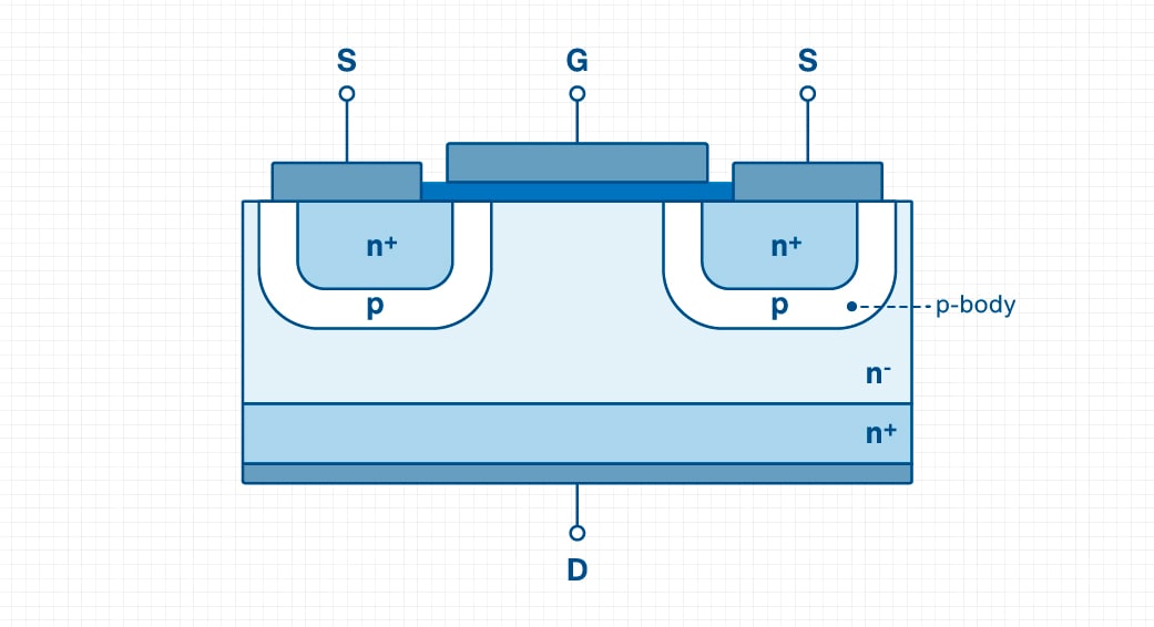
Figure 3: A structural diagram of a vertical silicon MOSFET. (Source: Mouser)
For an extensive comparison between these power switches and alternative technologies, consult the guide on whether to use MOSFETs or IGBTs for different power applications.
Silicon MOSFET Design Applications
MOSFETs in Switching Power Supplies
In switched-mode power supplies (SMPS), silicon MOSFETs serve as the primary power switches for converters. Modern high-efficiency converters often use synchronous rectification, replacing passive rectifier diodes with actively controlled MOSFETs to reduce conduction loss associated with diode forward-voltage (VF) drops. Selecting the right device requires balancing RDS(on) and gate charge (Qg) to optimise both conduction and switching losses for the target operating frequency.
Gate Drive Design for Switching MOSFET Applications
During switching, the gate driver must source and sink transient current to move the MOSFET’s gate charge, including the gate-to-drain charge associated with the Miller plateau. Datasheet gate-charge values are generally more useful than the internal capacitance (often represented by Ciss) alone for estimating driver current and switching time requirements. To satisfy these dynamic switching requirements while managing circuit parasitics, voltage offsets, and system safety, gate drive designs rely on several core circuit techniques:
- Gate resistors (Rg): Tuned to balance switching speed against electromagnetic interference (EMI) ringing caused by circuit parasitics.
- Galvanic isolation: High-voltage or safety-critical designs use optocouplers, pulse transformers, or digital isolators to protect low-voltage control circuitry.
- Bootstrap circuits: High-side N-channel MOSFETs require a gate-drive voltage above the switching-node voltage. A bootstrap diode-capacitor network is one common approach, although it requires periodic recharge and may not support continuous 100 percent duty-cycle operation without additional circuitry.
MOSFETs in Motor Control Applications
In motor control systems, silicon MOSFETs are arranged in H-bridge or three-phase inverter networks to drive AC or brushed and brushless DC motors (Figure 4). Achieving high efficiency requires selecting low-RDS(on) devices to minimise conduction losses, along with fast switching edges to minimise transition losses. Designers must provide an appropriate commutation path for inductive current using the bridge devices’ body diodes, actively controlled MOSFET channels, or external freewheeling diodes. Parasitic-inductance voltage overshoot may require additional voltage margin, optimized layout, snubbers, or clamps to keep the MOSFET within its drain-source voltage (VDS) and avalanche limits.
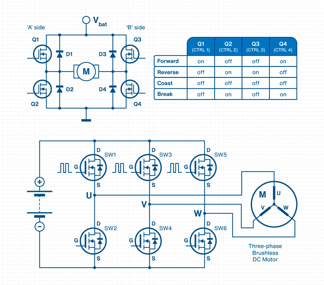
Figure 4: An H-bridge circuit (top) with four MOSFETs, flyback diodes, a DC motor, and an operational truth table. A three-phase BLDC inverter bridge (bottom) featuring six MOSFET switches, PWM control signals, and Wye-connected motor phases U, V, and W.
Figure 4: An H-bridge circuit (top) with four MOSFETs, flyback diodes, a DC motor, and an operational truth table. A three-phase BLDC inverter bridge (bottom) featuring six MOSFET switches, PWM control signals, and Wye-connected motor phases U, V, and W. (Source: Mouser)
For details on integrating motor drives, refer to the Basics of MOSFETs and IGBTs for Motor Control application analysis.
MOSFETs as Amplifiers
In amplifier circuits, a MOSFET is operated in its saturation region rather than as an on/off switch. Small changes in the gate-to-source voltage (VGS) produce corresponding changes in drain current, allowing the device to amplify analogue signals. This voltage-controlled behaviour makes MOSFETs widely used in audio amplifiers, RF amplifiers, and analogue signal-processing circuits.
For high-power linear applications, engineers often consider planar MOSFETs because they offer a more robust forward-biased safe operating area than trench devices, which are optimised primarily for switching. Device selection must nevertheless be based on the datasheet safe operating area, pulse duration, junction temperature, and thermal-stability limits.
MOSFETs in Power Management and Load Switching
In power distribution networks, silicon MOSFETs serve as highly efficient electronic switches for load sequencing, reverse-polarity protection, and hot-swap control. Combined with suitable control circuitry, a low-RDS(on) MOSFET can implement an ideal diode function, greatly reducing the voltage drop, power loss, and heat generation associated with conventional diodes.
MOSFETs are also widely used for power-path management. In redundant power supplies, MOSFETs can implement power-supply OR-ing, allowing multiple sources to feed a common rail while blocking reverse current into an inactive or failed source. They are also used for hot-swap and soft-start circuits where controlled gate drive limits inrush current when connecting large capacitive loads. Because the MOSFET may dissipate substantial power in linear operation during startup, its safe operating area must be verified for the expected voltage, current, pulse duration, and temperature.
Silicon MOSFET Selection Guide: Choosing the Right Device
Defining Application Requirements Before Selection
Selecting the right MOSFET begins with understanding the application’s electrical, thermal, mechanical, and environmental requirements. Key electrical parameters include voltage rating, current rating, RDS(on), switching speed, and gate-drive voltage. Thermal considerations determine the cooling strategy and package type, while environmental factors, such as vibration, shock, and operating temperature, may further influence device selection. Once engineers understand these requirements, they can choose a MOSFET technology and package that best suits the intended circuit topology.
Step-by-Step Silicon MOSFET Selection Process
For standard switching applications, MOSFET selection should follow a structured process that considers electrical, thermal, and reliability requirements:
- Define topology: Identify the MOSFET’s role (e.g., switch, driver) to set requirements.
- Determine voltage rating: Ensure the VDS rating allows sufficient margin for spikes and transients.
- Check current and conduction: Select RDS(on) using the root mean square (RMS) and peak currents, the available gate-drive voltage, the temperature-adjusted on-resistance, and the thermal budget.
- Confirm gate-drive capability: Verify that the driver provides the required VGS and can source and sink sufficient current to move the specified gate charge (Qg) within the target switching time.
- Analyse switching: Evaluate Qg, Miller charge, and capacitances (Coss/Crss) for efficient high-frequency performance.
- Evaluate body diode: Check reverse-recovery characteristics (trr/Qrr) for hard-switched or inductive circuits.
- Verify fault and transient capability: Check the safe operating area (SOA) for the applicable voltage, current, pulse duration, and temperature. Where avalanche may occur, evaluate the relevant avalanche-current and energy ratings under the datasheet test conditions, including any limits on repetitive operation.
- Validate thermal/package: Confirm heat dissipation maintains junction temperature (TJ) within safe limits.
- Simulate and test: Validate via Simulation Program with Integrated Circuit Emphasis (SPICE), then bench-test under real-world operating conditions.
How Does a MOSFET Compare to Alternatives?
Wide-bandgap semiconductors, such as gallium nitride (GaN) and silicon carbide (SiC), can operate more efficiently at higher voltages, switching frequencies, and temperatures than conventional silicon devices. These characteristics enable smaller, lighter, and higher-power-density systems. However, silicon MOSFETs benefit from a mature manufacturing ecosystem, lower cost, and widespread availability. As a result, silicon remains the dominant material in the global power semiconductor market, while silicon MOSFETs continue to be widely used in cost-sensitive and mass-market power-conversion applications.[1]
Conclusion
Silicon MOSFETs remain a foundational technology in modern electronic design, offering high input impedance, efficient switching performance, and a mature, cost-effective manufacturing ecosystem. By understanding their operating modes, device structures, and key datasheet parameters, engineers can make informed component selection decisions across applications ranging from power supplies and motor drives to load switching and analogue circuits. Despite the emergence of wide-bandgap technologies such as GaN and SiC, silicon MOSFETs remain the default choice for many power-conversion and control applications due to their availability, reliability, and cost-effectiveness.
To get started with a MOSFET project, explore Mouser’s extensive MOSFET selection.
Sources
[1]https://www.mordorintelligence.com/industry-reports/power-semiconductor-market