Advancing power supply solutions through the promise of GaN
By Texas Instruments
"Achieving more efficient electrical power conversion is a key technical goal in a world with a growing population and an ever-expanding need for energy."
One important innovation that promises to contribute significantly to meeting this goal is the use of gallium-nitride (GaN) in power applications. GaN is already an established semiconductor material, employed extensively in LED lighting and increasingly important in wireless applications. Now, with process advances and defect rate improvements, GaN is providing a number of advantages in electronic power supplies that convert electricity between alternating and direct current, change voltage levels and perform a number of functions to ensure the availability of reliable electric power.
The GaN-based switching power transistors that enable new power applications can operate at high voltages with much higher performance and lower losses than previously used silicon (Si) transistors. GaN characteristics, such as high-frequency operation, promote high performance while maintaining high efficiency. The GaN devices use a GaN-on-Si process that fits into the existing Si manufacturing flow. Given the much smaller size of the GaN device for the same current capabilities, the GaN transistor should eventually be as cost effective as its Si equivalent. This will make GaN devices attractive for systems ranging from huge industrial equipment to the smallest handheld devices. GaN will find its first home in higher-performance power designs because of its benefits. These designs are demanding as they push their operating frequencies and require precise switching characteristics. However, the promise of GaN for more efficient power conversion is steadily coming within reach.
Today, power supply designers are beginning to rethink their circuits, looking for ways to create power systems that can take full advantage of the new GaN transistors' potential, while avoiding unwanted effects. When considerations like these enter the picture, solutions are often found in the components themselves-GaN switches, Si switch drivers, high-speed switching controllers, and the power inductors, transformers and capacitors that are part of the overall design. Integrated circuit (IC) manufacturers who create power products can enhance the design possibilities considerably for customers by providing system-level solutions with co-designed devices, even to the point of integrating multiple chips in modular packages.
Texas Instruments (TI), the industry leader in IC solutions for power applications, is well-positioned to provide these types of solutions. With its innovative manufacturing processes, circuitry and packaging technologies, TI continues to supply devices that enable designers to get the most out of GaN.
GaN's place in the power supply chain
Most familiar electronic equipment operates from switched-mode power supplies (SMPSs), which efficiently convert alternating to direct current (AC to DC) and step-line voltages of 110-120 V or 220-240 V down to the 12-, 5-, 3.3-V and lower levels needed by system components. These functions are typical for consumer electronics and data centers, but SMPSs are also used for DC-to-DC conversion, and for higher voltage levels in inverters for renewable energy, as well as in automotive electronics, industrial equipments and other types of high-power systems.
Figure 1 shows the flow of a generalized SMPS. An input voltage, often AC at a high voltage and low frequency, is rectified to DC. Line filters serve to block the high frequencies developed in the power supply from transmitting back on the source line. A high-frequency power switch-the heart of the SMPS-converts the DC signal to a pulsed voltage waveform. The output from the switch is transformed to the needed voltage and filtered for a steady output at the level required by the low-voltage system. Feedback from the output is used by a controller to supply pulse-width-modulated (PWM) signals to the driver for the power switch, providing regulation. The pulse width of the signal is increased or decreased as load requirements change.

Figure 1: Generic functions of a switched-mode power supply.
Traditionally, power switches have been silicon MOSFETs (metal-on-silicon field-effect transistors), but are now being replaced by GaN FETs.
Depending on system requirements, a wide variety of design topologies can be used and will require various arrangements of power switches, from single-FET boost converters, through a number of two-FET designs, up to four-FET full-bridge converters. The switch and its driver form an extremely sensitive area of the design as they must perform precisely as the controller is commanding. If they do not, the power system becomes unstable. Additionally, because of rapid rise and fall times of the modulated voltages, noise can be injected to the feedback loop that may result in an unstable power system.
One requirement for all grid-connected systems is isolation between what comes from the grid and what is supplied to the system, providing safety for the downstream equipment. Another concern is that high-frequency operation of the power conversion must not be allowed to interfere with power delivered by the grid and create noise on the source power line. GaN devices address this isolation requirement and need to reduce electromagnetic interference by allowing higher frequency operation. This higher frequency can reduce the size of the isolation transformer and input filter.
Advantages of GaN for SMPS systems
GaN has important advantages over silicon for power supply switching because it offers lower losses at higher voltages. It also uses less energy to turn on and off. Si switches have improved greatly over the years, but for the same size and high voltage, GaN offers a significant improvement that is unlikely to be matched by Si. Today, Si MOSFETs have a sizeable cost advantage over GaN, but over time that cost differential will be reduced.
GaN switching devices are offered over a wide range of operating voltages. They offer power designers the opportunity to reduce the physical size of their solution by operating at higher switching frequencies while maintaining desired efficiencies for a very large range of input and output voltages. Applications where GaN is most valuable tend to be those where the power solution needs to be miniaturized as much as possible.
Figure 2 shows the basic structure of a GaN transistor. As discussed earlier, the GaN material is on a Si substrate. By doing this we get the advantage of the decades of Si processing while we also get the advantage of GaN. One benefit comes from the higher band gap voltage.
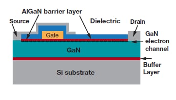
Figure 2: Cross section of an enhancement mode GaN FET.
Semiconductors exist as a class of materials because of band gap energy-the jump in voltage required to change the material from an insulator to a conductor. The band gap energy of 3.2 electron-volts (eV) that GaN offers is nearly three times that of Si. Theoretically, this higher band gap means better performance at higher temperatures, because more heat can be sustained before the substance becomes conductive. In the future, this feature may improve GaN performance in automotive, industrial and other high-temperature environments.
The GaN learning curve in SMPS design
For the many advantages GaN offers, the technology is just beginning to find its way into power supply design. Previous uses of GaN in LEDs and wireless applications might give the impression that the technology was ready for power supplies, too. But, in fact, significant process and device development was required to use GaN in power FETs and have slowed product development. Moreover, differences in new FETs from their Si predecessors have compelled IC suppliers and system designers to proceed carefully, resolving design complexities issue by issue. Traditional GaN devices are normally on, or in depletion mode, whereas Si MOSFETs are enhancement- mode devices that are normally off. In order to provide drop-in replacements for Si MOSFETs, GaN FET switch suppliers either redesigned their products to operate in enhancement mode or used another switch in series to provide the normally off functionality.
Replacing a Si MOSFET with a GaN FET is only the beginning of the redesign. The higher frequency capability of a GaN transistor demands greater timing precision in the switch driving signal, and the switches are highly sensitive to parasitic impedances from packages, interconnect and outside sources. Integrated Si-based GaN drivers that turn GaN switches on and off at high speeds have helped move GaN-enabled SMPS design along. Mature Si processes enable the development of these extremely precise, high-frequency tunable drivers. For example, TI's LM5113 gate driver was created to control high- and low-side enhancement-mode GaN power switches at medium voltage levels. The gate driver integrates the required components to optimize the performance of GaN switches. This integration not only reduces board space but also helps simplify the design. In addition to achieving high-precision drive timing with minimal delay, the device also provides important protections for the efficient, precise operation of the GaN switch. For example, bootstrap clamping keeps the gate-to-source voltage in a safe operating area; a high-current pull-down improves dv/dt immunity and prevents accidental activation of the low side; independent source and sink pins allow optimization of turn-on and turn-off times for efficiency and low noise; and fast propagation delay matching optimizes dead times when the switch is in transition.
System-level solutions for GaN-based SMPS design
Combined in use with fast, precise power management control, GaN gate drivers have considerably advanced GaN-based SMPS design. However, the gate drivers by themselves are limited in how much optimization they can offer. Even the shortest possible traces between the driver and the GaN switch give rise to delays that vary according to the design.
Future IC solutions will need to control variability issues resulting from the layout and design of passive components, since these are all-important in coupling the driver and switch. Because the two devices are based on different materials with widely different properties, they probably will not be integrated economically in a single chip (die) in the near future. However, a single-package module (Figure 3) that integrates the FETs, driver and passive devices supporting the switch would considerably reduce the area and component count of the SMPS. This size reduction would also mean a reduction in system manufacturing costs, along with the increased efficiency of GaN-based design.
Just as important as scaling down the solution is decreasing design complexity. A driver-switch module would reduce inter-chip connections to the shortest possible lengths, minimizing the delay times and parasitic impedances that serve to distort the pulsed output of the switch. A well-designed module could reduce the parasitic factors of a multi-chip design considerably, some of them by an order of magnitude or more.
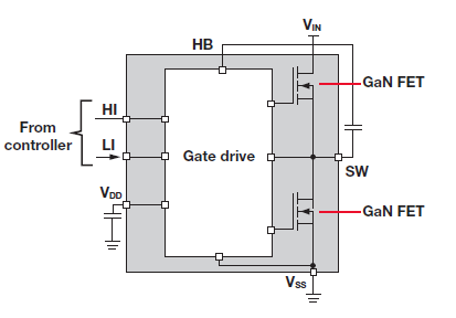
Figure 3: Integrated GaN switch-gate driver module.
Another important factor in supplying system-level solutions is the controller-regulator, which has to operate at the higher frequencies enabled by GaN. This device must respond to changes in the output voltages in real time. The time resolution must also meet the precise pulse width requirements to minimize conduction losses during the dead time. Fortunately, digital power controllers are available to support these requirements, offering additional performance and I/O functions that can be used elsewhere in the system. TI offers in-depth expertise in digital power control, which combines with the company's power supply technology to provide system-level solutions for GaN regulation and controlled switching.
Also needed are magnetics for GaN-based designs, since these components are still scaled for silicon-enabled frequencies. TI collaborates with power supply manufacturers and GaN research institutions to continuously press magnetics suppliers for these components, but much depends on the market. As GaN-based power component availability and volume increases, magnetics suppliers will get volume requests from their customers to introduce components scaled for the technology. Once these and other enabling factors are in place, the industry will be able to leverage the benefits of GaN in many power supply applications.
GaN innovation for tomorrow's needs
The world's growing population and rising development create an ever-increasing demand for electricity, while environmental issues increase the need to do more with less energy. As we try to address these needs, the world will benefit from innovations that help us deliver, convert and consume electrical power more efficiently, resulting in technologies that improve and enhance our lives.
GaN is one such innovation that promises to help us get more out of our energy resources by minimizing power losses in electrical conversion. Rising to GaN's challenges, TI is leveraging its leadership in power and commitment to research and development to create solutions that reduce the complications that arise with high-frequency power conversion. These differentiated solutions will help to simplify design, save space and reduce component counts while minimizing the signal delays and stray interferences that reduce efficient operation.
As products appear that offer these advantages, SMPS developers will be able to design higher-performance systems at a faster time-to-market. The success of these systems will push GaN into new application areas, both at the high-power, industrial end of the scale and at the low-power, mass-market end. Modules and other key parts of system-level solutions will help us realize the full potential that GaN technology offers in power supply efficiency.