RF Power Amplifier Efficiency: A Crucial Metric for 5G and IoT
Five years from now, the wireless industry as we know it today may be almost completely transformed. Cellular networks that have always relied mostly on “macro” base stations will be supplemented with hundreds of thousands of “small cells.” Wireless-enabled sensors with tiny battery-operated transceivers will be deployed by the billions to make the Internet of Things a reality. And wireless carriers will use operating frequencies well into the millimeter-wave region of the spectrum where only a few applications operate today.
If there is a common theme in this scenario, it’s the need for RF power transistors and amplifiers to achieve the highest possible efficiency, as the transmit section of any transceiver contributes significantly to overall operating costs, as is shown in Figure 1. Obviously, no device that generates RF power can achieve 100% efficiency, as there are too many impediments to converting DC power into RF power, from losses incurred throughout the signal path, to operating frequency, the inherent characteristics of the device, to name a few.
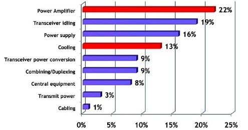
Figure 1: RF-related components contribute significantly to the power consumption of a cellular base station.
Nevertheless, even incremental increases in efficiency reap rewards such as reduced power consumption and potentially fewer devices required to deliver a specific RF output (and thus a smaller overall amplifier footprint). And in cells and IoT devices reducing power consumption is crucial. So it shouldn’t come as a surprise that manufacturers of RF power transistors, RF Integrated Circuits (RFICs), and Monolithic Microwave Integrated Circuits (MMICs), as well as academic institutions, are working hard to increase efficiency. The result is a trend toward increasing RF efficiency at the device level as well as through the use of techniques such as envelope tracking, digital pre-distortion/crest factor reduction schemes, and higher classes of amplifiers beyond the ubiquitous Class AB.
An excellent example of the current efficiency potential of GaN technology is Wolfspeed’s CGHV14800F GaN HEMT power transistor (Figure 2). Although it is conservatively rated to deliver 800 W between 1200 and 1400 MHz, typical performance (with a pulse width of 100 µs and 5% duty cycle) ranges from 910 W at 1400 MHz with efficiency of 67% to 1 kW at 1200 MHz with efficiency of 74%. The transistor is designed for use in L-band radars for air traffic control, weather, antimissile systems, target tracking, and long-range surveillance.
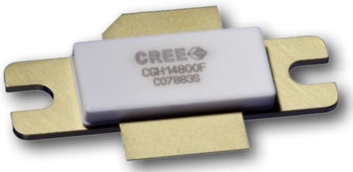
Figure 2: The CGHV14800F GaN HEMT from Wolfspeed achieves extremely high efficiency up to 74% and RF output power of 1 kW at L-band.
Mr. Doherty’s Comeback
A significant change in amplifier design that is now almost universally used in base station amplifiers is the Doherty architecture. It was invented in 1936 by W.H. Doherty of Bell Labs (then a part of Western Electric), and produced an amplifier that can deliver very high power-added efficiency with input signals that have high peak-to-average ratios (PARs). When properly designed, a Doherty amplifier can increase efficiency by 11% to 14% when compared to standard parallel Class AB amplifiers.
However, the Doherty was a nearly dormant invention for many years as the modulation schemes employed in communication systems were AM and FM and only a very few signal types possessed characteristics for which the Doherty was well suited. Today virtually every wireless system produces high-PAR signals, from WCDMA to CDMA 2000, and any system employing Orthogonal Frequency Division Multiplexing (OFDM), such as LTE and Wi-Fi.
A classic Doherty amplifier (Figure 3), which falls into the class of load modulation architectures, actually consists of two amplifiers: a carrier amplifier biased to operate in Class AB mode, and a peaking amplifier biased to operate in Class C mode. A power divider splits the input signal equally to each amplifier with a 90-deg. difference in phase. After amplification, the signals are rejoined with a power combiner. Both amplifiers operate during the peaks of the input signal and are each presented with a load impedance that enables maximum power output.
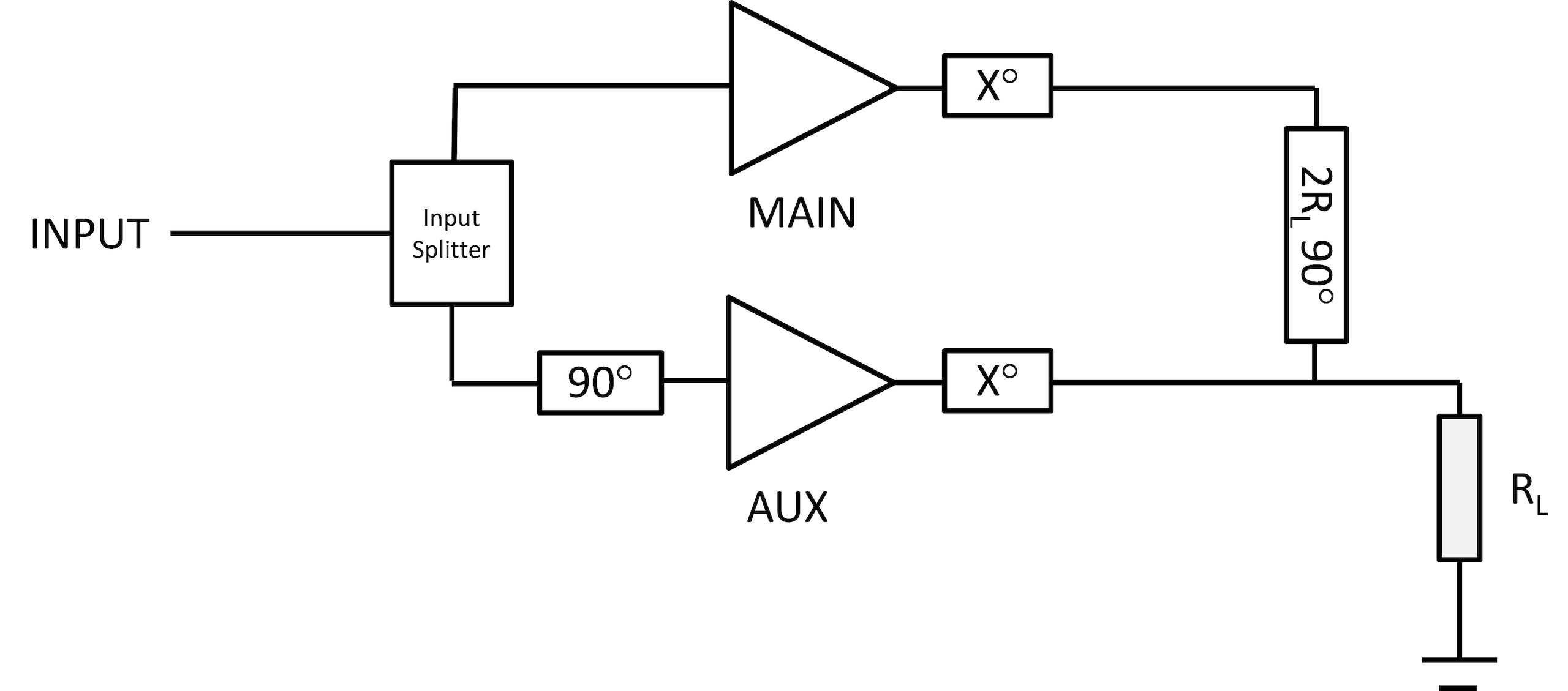
Figure 3: A single-ended Class AB, two-way Doherty amplifier. Source: Slipstream Engineering Design Ltd.
As the input signal power decreases, the Class C peaking amplifier turns off and only the Class AB carrier operates. At these lower power levels, the Class AB carrier amplifier is presented with a modulated load impedance that enables higher efficiency and gain to be produced. Advances in Doherty amplifier design have been made in rapid succession as the architecture has been rejuvenated, which has led to its current success.
The Need for Linearization
Of course, no architecture is perfect and linearity is somewhat less in a Doherty amplifier than in a dual Class AB amplifier, so analog and digital linearization techniques are required to improve it. The most widely used today is digital predistortion (DPD) sometimes in combination with crest factor reduction (CFR). Both DPD and CFR dramatically reduce the Doherty's distortion and careful device and amplifier design can minimize the reduction in linearity. However, their use is not strictly defined to use in Doherty amplifiers, as benefits are achievable in other amplifier architectures as well.
Unfortunately, amplifiers perform best when they are driven near their saturation point, after which they become nonlinear and RF power output begins to decrease with increases in input power. In addition, significant distortion begins to appear that can cause interference to adjacent channels or services. As a result, designers typically back off RF output power into a "safe zone" to ensure linearity. When they do that, more RF transistors are required to deliver a given RF output power, which in turn increases current consumption and results in less battery life or in a base station, higher operating costs.
DPD effectively introduces "inverse distortion" into the amplifier's input, canceling the amplifier's nonlinearities. The result is that the amplifier need not be backed-off from its optimum operating point, potentially negating the need for more RF power devices. As the amplifier is more efficient, benefits are obtained in both reduction of cooling overhead and in all-important power consumption. CFR also functions to keep a check on distortion by reducing the peak-to-average ratio of the input signals, reducing signal peaks so that the signal can pass through the amplifier without clipping or distortion. When DPD and CFR are used together, even greater benefits can be achieved.
The Outphasing Approach
Another amplifier architecture developed and patented nearly 80 years ago by Henri Chireix is called "outphasing" and has demonstrated its ability to increase amplifier efficiency and increase operating bandwidth. In general, the approach controls the phase shift of multiple saturated or switched-mode RF power amplifiers to create a modulated RF output. A lossless, non-isolating power combiner produces load modulation of the amplifiers that modulates the output. As it can increase efficiency over a broad range of power levels, it us well suited for use in today’s high-PAR communication systems.
Research into the outphasing approach has been conducted by both device manufacturers and academia to eliminate some of its disadvantages, perhaps the most important of which is the need to separate the signal into multiple phase-and amplitude-modulated signals. This increases the number of required components (and thus cost) when compared with the Doherty approach that does not need this separation. However, ongoing research is mitigating these problems, potentially making it an excellent complement to the Doherty amplifier.
Envelope Tracking
Still another arrow in the quiver of amplifier designers is envelope tracking, in which the voltage applied to the power amplifier is continuously adjusted to make sure that it is operating in its peak operating region and thus at maximum power. It is the evolution of an earlier technique called envelope elimination and restoration (EER) that was proposed by L. R. Kahn in 1952 (commonly called the “Kahn method”) and has been the subject of considerable research ever since.
With envelope tracking, the power supply voltage applied to the amplifier is continuously adjusted so that it always operates at peak efficiency, in contrast to more conventional amplifier design techniques in which a fixed supply voltage operates most efficiently only when operating in compression. The latter type decreases in efficiency with increases in crest factor as the amplifier operates mostly below its peak power level and thus its maximum potential efficiency.
Envelope information employed by envelope tracking is based on the characteristics of the I/Q modem and is sent to a specialized power supply in order to provide the required voltage. The technique was first incorporated in a chip by Qualcomm in 2013 and is now widely used in smartphones from many manufacturers. Like all techniques, envelope tracking has limitations, one of the most important being limited signal bandwidth of 20 to 40 MHz, which presents problems as wireless access methods have increased over the years from a few megahertz to nearly 100 MHz in LTE-Advanced and 160 MHz in IEEE 802-11ac.
However, a recent development called Envelope Tracking Advanced (ETAdvanced) seems to have mitigated this problem and. It was created and patented by a spinoff from Massachusetts Institute of Technology called Eta Devices founded by MIT engineering professors David J. Perreault and Joel Dawson who developed Asymmetrical Multilevel Outphasing (AMO) after 10 years of research on which ETAdvanced is based. The company is funded by Stata Venture Partners whose cofounder is Ray Stata who also cofounded Analog Devices. Cofounders include Mattias Astrom, a serial entrepreneur, and Dr. Mark Briffa, a lead researcher and designer at both Huawei and Ericsson. It was acquired last October by Nokia.
The company says ETAdvanced allows base station transmitters to achieve the highest efficiency at peak power and back-off of any other technique. For narrowband applications, ETAdvanced is 25% more efficient than envelope tracking using fewer components in a less complex design. It also accommodates channel bandwidths up to 160 MHz making it useful for both LTE-Advanced, 802.11ac Wi-Fi, and potentially systems incorporated within the fifth-generation of wireless, 5G.
At European Microwave Week last October the company demonstrated an 802.11ac Wi-Fi RF power amplifier controlled by ETAdvanced that consumes 80% less power than a typical amplifier for this application, over a channel bandwidth of 160 MHz. The company says it represents the first time an advanced supply-modulation technology has been demonstrated for an application with very broad bandwidths.
Summary
Work being conducted into increasing the efficiency of RF power generation, if described completely, could fill a large book. Efforts are underway not only in the areas discussed in this article but in the use of different classes of amplifiers and assorted techniques that are combined to produce interesting results. Regardless of how these advances are achieved, one certainty is that the search for higher and higher efficiency will continue for as long as there is demand for ever higher data rates.