Wide Bandgap Semiconductors Tackle Tomorrow's Systems
Wide bandgap semiconductors are about to redefine what can be achieved in applications from electricity-powered vehicles to radar and powering the grid, leapfrogging over traditional semiconductor technologies to deliver higher performance at higher voltages and output power, and operating frequency in smaller packages.
It's hardly news that the properties of wide bandgap (WBG) materials such as gallium nitride (GaN), silicon carbide (SiC), and diamond are reshaping applications ranging from power electronics to lighting and generation of RF and microwave power. However, the pace at which this is occurring is actually matching or even exceeding analyst projections of only a few years ago. As WBG properties are amazingly well matched to applications that are important today and will continue to be long into the future, it’s a very good time to be in the WBG semiconductor business and all the way up the product “food chain” to the system level.
For starters, WBG devices can eliminate up to 90% of the power losses that currently occur during AC-to-DC and DC-to-AC electricity conversion, operate at voltages up to 10 times higher than silicon-based devices, and operate at temperatures above 300°C, twice what silicon devices can tolerate. When employed in the RF and microwave domain, they can operate at higher frequencies at higher RF output powers and over wider bandwidths: up to 10 times higher in frequency than silicon-based devices and higher RF output power than GaAs at higher frequencies. When LEDS are employed to replace incandescent and fluorescent bulbs, they can produce more than 10 times the light per watt of input energy and extend service life by at least 30 times, and when GaN is combined with indium as (InGaN) or aluminum (AlGaN) it allows LEDs to produce a color range from red to ultra-violet.
The Department of Energy predicts that WBG-based, low-cost, high-performance power electronics will be employed in everything from household appliances and consumer goods to military systems, vehicles, and a modernized power grid that incorporates renewable energy. The WBG share of the global lighting market alone is projected to reach $84 billion by 2020, according to DoE, and GaN and SiC are expected to claim 22% of the $15 billion global market for discrete power electronic components by 2020 in buildings and industrial, electronics and IT, renewables and grid storage, and transportation alone.
Bandgap in Perspective
For those not familiar with WBG semiconductor technology it's not the least bit surprising, as understanding it requires a deep dive into solid-state physics. From an admittedly superficial perspective, electrons in a solid exist at energy levels that combine to form energy bands (Figure 1).

Figure 1: Bandgaps are the key to defining the difference between insulators, conductors, and semiconductors. Source: http://commons.wikimedia.org/wiki/File:Band_gap_comparison.svg
The top band is called the conduction band and a next lower one is called the valence band (there are others as well). The region between the valence band and the conduction band is the bandgap.
If the electrons in the valence band are externally excited they can move up to the conduction band if they have enough energy. A conductor (copper, for example) has no bandgap as the two energy bands overlap. An insulating material has a gap so wide that it takes too much energy to bridge it. A semiconductor is much closer to a conductor (thus the name “semi” conductor) and allows certain amounts of energy to cross between the valance and conduction bands.
The amount of that energy determines where in the bandgap hierarchy a semiconductor falls. The reference material is usually silicon as it has a bandgap of 1.1 electron volts (eV) or gallium arsenide (1.4 eV). In comparison, GaN has a bandgap of 3.4 eV, SiC 3 eV, and diamond 5.5 eV. The benefits of this characteristic are significant as it separates a WBG material from others in its ability to operate at much higher temperatures, voltages, and frequencies. Some or all of these properties are invaluable in specific applications.
Even the White House has joined the WBG bandwagon, in January announcing that North Carolina State University will lead the Department of energy’s manufacturing innovation institute for the next generation of power electronics. The university will work to drive down costs of and “build America’s manufacturing leadership in wide-bandgap semiconductor-based power electronics -- leading to more affordable products for businesses and consumers, billions of dollars in energy savings and high-quality U.S. manufacturing jobs.”
The implications of WGB are already positively affecting high-power electronics employed in everything from industrial motors to power supplies, inverters for converting solar and wind energy into AC electricity, utilities (where they can reduce transformer size), converters and other uses in electric and plug-in hybrid vehicles, and geothermal power generation (where extremely high temperatures are encountered). As GaN is a key component of LEDs lighting, its future in this market is assured, and last but not least is the generation of high levels of RF and microwave power using solid-state devices rather than vacuum tubes (such as traveling-wave tubes).
Power Electronics
The extraordinary advantage of WBG materials in handling very high voltage could not be better expressed than in (Figure 2) from eVince Technology, which compares the amount of material required to isolate 10,000 V.
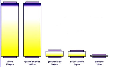
Figure 2: WBG semiconductors have extraordinary potential to handle high power, in this case for isolating 10 kV. Source: eVince Technology http://www.evincetechnology.com/whydiamond.html
This is obviously most important in industrial applications and especially those in which the highest voltages must be accommodated from scientific research to electrical power transmission. As a much smaller amount of material is required to accomplish a specific task such as power conversion the benefits are obvious: smaller size, greater efficiency, and higher reliability, to name just a few.
A good example of how important WBG devices will be in the future is the power converters used as rectifiers, power supplies, and battery chargers in transportation applications, and especially in electric and hybrid electric vehicles (HEVs). In both scenarios, these devices must be compact, lightweight, have high power density and efficiency, and operate reliably for very long periods under harsh conditions. However, electric vehicles and HEVs employ an electrical traction drive that carries the most power among all the vehicle’s power converters. As heat in an HEV is generated by the engine, the motor, the semiconductor device losses, and the environment, the electronics must be cooled. The maximum junction temperature limit for most silicon devices is 150°C and the variation in their electrical characteristics with temperature and time is a reliability issue.
Ambient air, forced air, or water-cooled heat sinks could be employed to keep temperatures under control, but high-power converters require liquid-cooled heat sinks that are fairly complex, large, and heavy - the antithesis of what an HEV needs. Insulated gate bipolar transistors (IGBT) and PIN diodes are used in converters but have higher losses compared to MOSFET and Schottky diodes and are not used in traction drives because they are not available with high power ratings. Higher-voltage- silicon (but not SiC) MOSFETs and Schottky diodes, while delivering good performance, are not feasible because as their breakdown voltage increases their silicon die area increases, reducing manufacturing yields and increasing cost. Consequently, a material with a higher electric breakdown field is required.
In short, silicon has reached its theoretical temperature limit, making it of less and less interest and use in transportation applications and other in the future. WBG semiconductor power devices can work in harsh environments where silicon power devices cannot function. They are thinner and have lower on-resistances resulting in lower conduction losses and higher overall converter efficiency. They also have much higher breakdown voltages because of their higher electric breakdown field, so while silicon Schottky diodes typically have breakdown voltages up to 300 V, SiC Schottky diodes achieve in excess of 600 V.
For example, the 650-VDC IDH03G65C5, part of Infineon Technologies’ ThinQ!™ Generation 5 family of SiC Schottky barrier diodes, offers improved efficiency over all load conditions, thanks to improved thermal characteristics and a lower figure of merit. It is designed to handle high-temperature conditions, has no reverse of forward recovery, switching behavior independent of temperature, high surge current capability, and is breakdown voltage tested at 6.8 mA.
WBG devices also have higher thermal conductivity and a lower junction-to-case thermal resistance so heat is more easily removed from the device (except for GaN, which will be discussed later). As WBG devices can operate at higher temperatures, their forward and reverse characteristics vary little with temperature and time (reducing the reliability issue), generate less electromagnetic interference (EMI).
The Wolfspeed CAS100H12AM1 1200V high-frequency half-bridge module exemplifies the next generation of SiC power modules. It is the first commercially available all-SiC power module and the first qualified module with both SiC MOSFETs and SiC Schottky diodes combined in a single half-bridge package. It has very low loss, is extremely rugged, operates up to 100 kHz, and provides 100 A current handling at 1200 V blocking. It is designed for used in power converters, motor drives, solar inverters, UPS and SMPS, and induction heating.
Solid-state Generation of RF Power
Over the entire history of the RF and microwave industry, the highest level of RF power has been generated by vacuum tubes, as solid-state devices could deliver only a tiny fraction of the kilowatts (or even megawatts) that these “vacuum electron devices” could produce. At the highest power levels, this situation won’t change for decades at the very least, but GaN has the potential to reach the lower levels of “high-power RF”. It will also do so at higher frequencies than any other competing semiconductor technology, along with the ability to operate at higher voltages and thus higher efficiency, as well as several other advantages.
One of GaN’s key benefits is its power density (the amount of power that can be generated per unit of die size), which is significantly higher than that of its counterparts. For example, silicon devices have a power density of 0.2 W/mm, and GaAs reaches about 1 W/mm. In contrast, GaN has a (theoretical) power density of more than 30 W/mm and SiC with which GaN is often combined as a substrate material is 10 W/mm. It must be pointed out that GaN-on-SiC devices have a long way to go before they achieve 30 W/mm. Current devices deliver, according to most public sources, no greater than about 11 W/mm, which is still a formidable number as the technology is steadily advancing and is relatively new when compared to silicon and GaAs.
In practical terms, this level of power density means that more power can be generated by fewer devices, each of which has a much smaller die area, resulting in high-power RF amplifiers that are smaller, lighter, and more efficient. For example, Raytheon states that when compared to GaAs MMICs that are currently used, an Active Electronically Scanned Array (AESA) search radar can achieve five times the search volume in the same amount of time and 50% greater range with the same sensitivity using an antenna array size 50% smaller.
MACOM’s MAGX-001090-600L00 GaN-on-SiC HEMT RF power transistor is one of the industry’s best examples of what GaN can currently achieve. The 32-VDC packaged device delivers 600 W of peak power (32 μs pulse, 2% duty cycle) from 1030 to 1090 MHz, making it very appealing for L-band secondary radar, air traffic control, Mode-S transponders, and military IFF and data links. It has gain of at least 20.8 dB, and efficiency of between 58.6 and 64.4%.
In addition, TriQuint Semiconductor’s broadband 48-VDC GaN on SiC TGA2216 GaN RF power amplifier delivers P1dB RF output from 300 MHz to 3 GHz of +34 dBm (2.5 W) with 14 dB of gain and greater than 40% power-added efficiency. Its broad bandwidth makes it well suited for applications ranging from communications to radar.
In short, GaN will expand its reach into electronic warfare, wireless communications (both commercial and military), and other RF and microwave applications, making it, as has often been stated, the “technology of the future”. Nevertheless, while GaN is the fair-haired boy of RF power, the very power density from which it gains so much of its prowess also produces prodigious amounts of heat that must be transferred form the device in the most efficient possible way, which brings us to another WBG material: diamond.
Why Diamond
It might seem odd to include diamond in a discussion of semiconductors, but it is also a WBG material, is compatible with GaN and SiC, and has one characteristic that makes it unique: Industrial-grade polycrystalline diamond (a lot less expensive than raw diamond) has the highest thermal conductivity (ability to transfer heat) of any material on Earth, ranging from 1200 to 2000 W/mk. Consequently, it may play a key role in allowing WBG semiconductors to achieve their promise in RF and microwave power generation and other applications. When combined with aluminum particles to create aluminum diamond metal matrix composites (MMCs) they can be used in the heat spreaders at the base of GaN-based discrete RF power transistors and Monolithic Microwave Integrated Circuits (MMICs).
An aluminum diamond MMC retains diamond’s conductivity of about 550 W/mK, far higher than common heat spreader materials such as copper tungsten (200 W/mK), copper molybdenum (250 W/mK), and copper-molybdenum-copper (350 W/mK) that are used in the vast majority of current RF power transistors - including GaN -- as a heat spreader material (Figure 3).
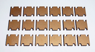
Figure 3: Aluminum diamond MMC heat spreaders. Source: Nano Materials International, Inc.
As the cost of aluminum diamond MMCs is somewhat higher than traditional materials, it's not likely to be widely used in low-power GaN devices, but as GaN's power density rises so does the heat dissipation challenge, making it very appealing at the highest RF power levels in which heat dissipation becomes far more difficult.
Summary
Making projections about the future of wide bandgap materials is relatively easy: It will thrive, not just for the next few years but for decades to come, replacing not just silicon but other semiconductor technologies as well in many applications. Confidence in making such a projection is made easier by the fact that so many different systems in so many markets- most of which are enormous- need what these semiconductor materials can provide.