Terasic FPGA Cloud Connectivity Kit: Part One

Image Source: Scharfsinn/Shutterstock.com
By Mouser Staff
Published November 22, 2021
Introduction
The ability to monitor and measure parameters at the edge is important, and the ability to communicate that information from the edge to the cloud for further processing and analysis is critical for many applications.
In this project we are going to look at how we can measure soil quality, which is important for sustainable agriculture, using hardware outlined in the Bill of Materials listed below:
In part one of this project, we are going to create the edge-based solution, which measures the soil quality using an embedded Linux solution.
Bill of Materials
The following are used to create this project:
- Terasic Technologies FPGA Cloud Connectivity Kit: 993-P0685
- Analog Devices Inc. EVAL-CN0398-ARDZ Evaluation Board: 584-EVAL-CN0398-ARDZ
- DFRobot Analog Waterproof Capacitive Soil Moisture Sensor: 426-SEN0308
- DFRobot Analog Spear Tip pH Sensor / Meter Kit: 426-SEN0249
Architecture
The Analog Devices CN0398 Evaluation board connects to the Terasic cloud connectivity board via the Arduino Uno R3 compatible expansion headeras shown in Figure 1.

Figure 1: Intel DE10 Nano and assembled with the Shield (right) (Source Mouser)
To be able to connect to the Microsoft Azure servers, we will be running an embedded Linux solution on the Hard Processor System (HPS), while the connectivity to the necessary pins on the Arduino shield will be made via the FPGA Fabric.
At the electrical level the AD7124 ADC, which is used to perform the measurements, uses a SPI interface. In addition to the SPI interface, there is also an enable pin required to enable the power supplies on the Analog Devices shield. These connections are demonstrated in Figures 2 and 3.
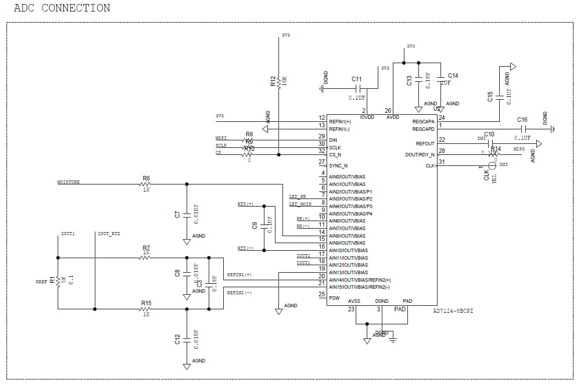
Figure 2: ADC Interface (Source ADI)
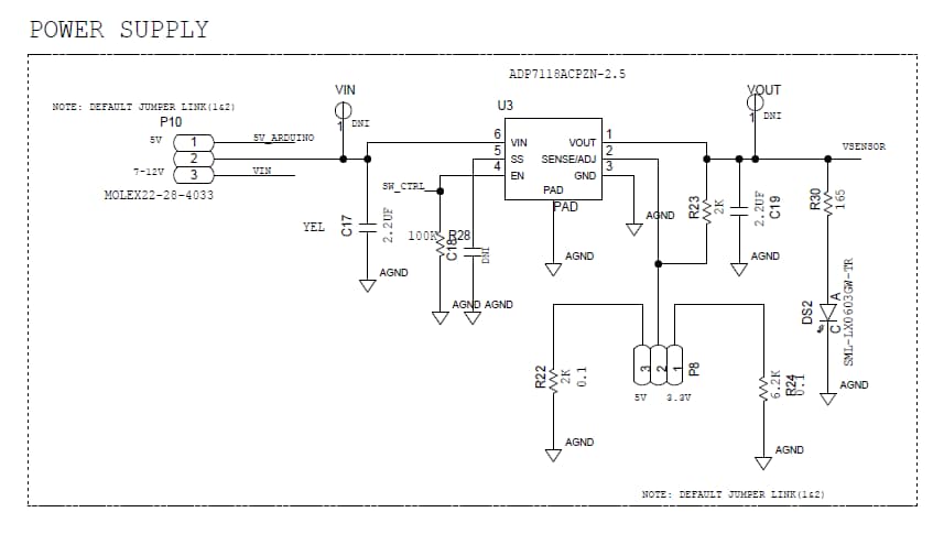
Figure 3: Power Interface (Source ADI)
Embedded Linux Solution
The embedded Linux solution which is running on the HPS must be Ubuntu 18.04 to be able to support the connection to Microsoft Azure services. The SD Card image for Ubuntu 18.04 can be found Download the file and write it to an SD Card using either BaleaaEtcher or RUFUS .
We can now get started looking at creating the overlay and device tree for the FPGA Fabric interfacing and the necessary drivers from the Linux kernel. This includes using the Industrial Input Output drivers, which support working with the AD7124 ADC.
Creating the Overlay
The first step on this journey is to clone or download the repository here https://github.com/intel-iot-devkit/terasic-de10-nano-kit
This project is one example project of the DE10 Nano tutorials; we will use this as a base for our developments.
The main functionality of this new overlay is very simple—we want to connect the HPS SPI pins to the Arduino header pins shown in Figure 4. In the current design, they are connected to dedicated HPS IO, which are rooted on the DE10 Nano board to the LTC Connector J17.
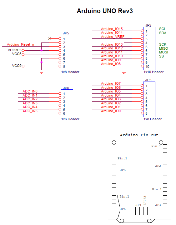
Figure 4: DE10-Nano Connections (Source Intel)
We also need to enable the power regulator; for this we are going to tie the output high, permanently enabling the power supply.
To get started with the modification, the first thing we need to do is open a project in the repository just cloned. The project to open is located under the directory path
<download location>/terasic-de10-nano-kit\azure-de10nano-document\sensor-aggregation-reference-design-for-azure\hw\Module5_Sample_HW
Using Quartus Lite select File->Open Project and select the Module5_Sample_HW.qpf as shown in Figure 5 will open the project in Quartus.
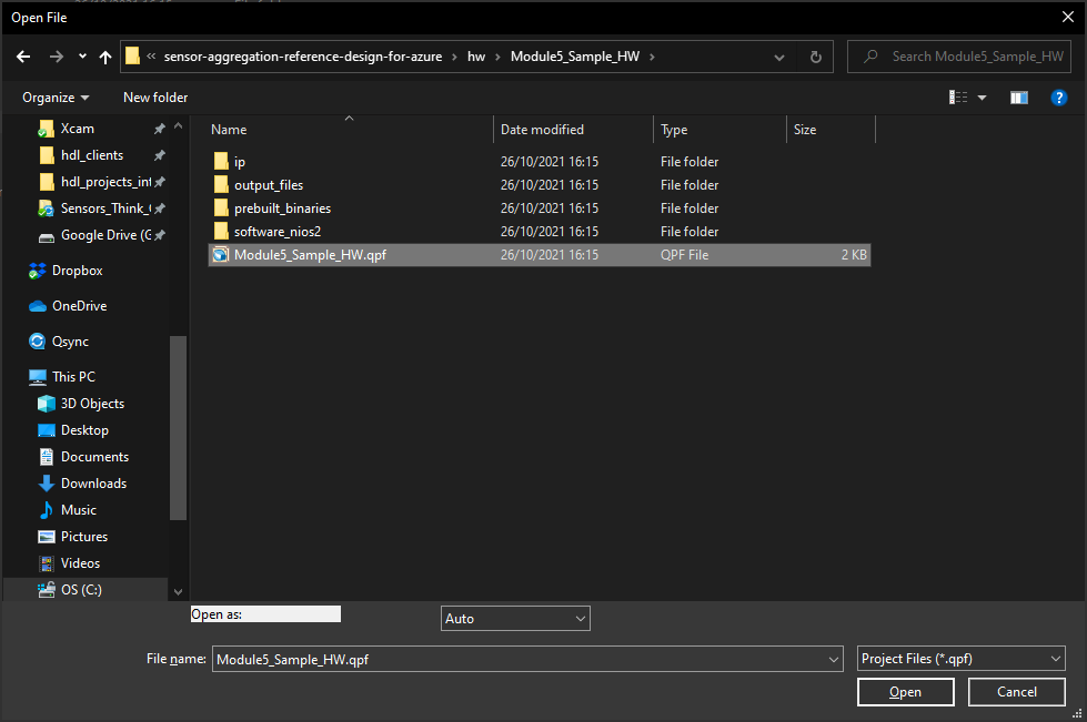
Figure 5: Opening the existing project (Source Mouser)
Once the project is open (Figure 6), we need to open Platform Designer to be able to modify the SoC design in the project and route the signals appropriately.
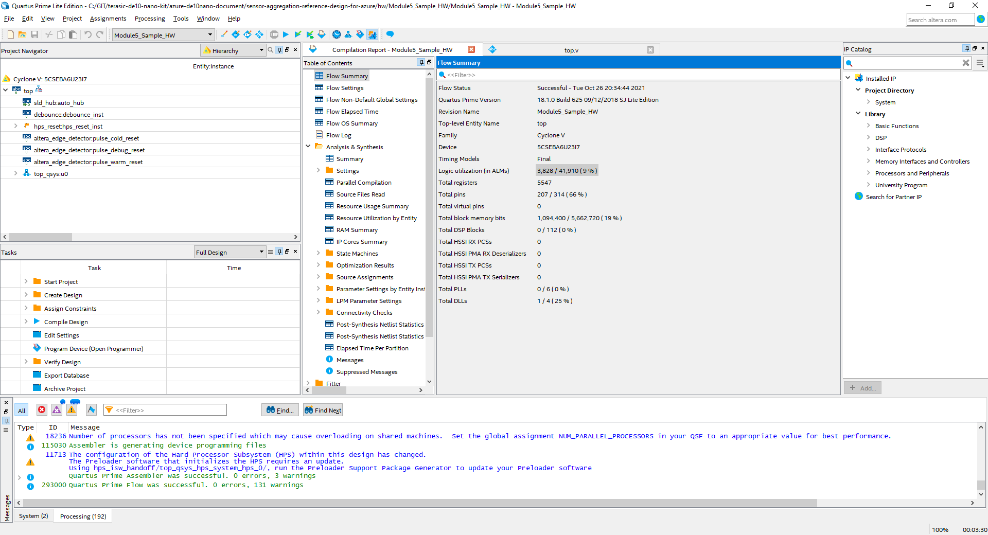
Figure 6: Quartus Project Open (Source Mouser)
Platform designer can be opened by selecting Tools->Platform designer in Quartus. Once Platform Designer opens, select the file top_qsys.qsys as shown in Figure 7.
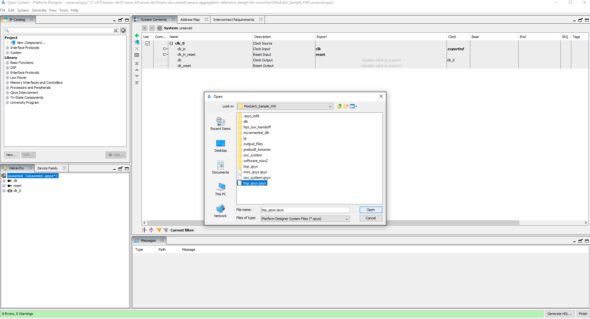
Figure 7: Opening the QSYS Design (Source Mouser)
This will open the entire reference design, which comprises the HPS and a NIOS subsystem, which is implemented in the FPGA Fabric (Figure 8).
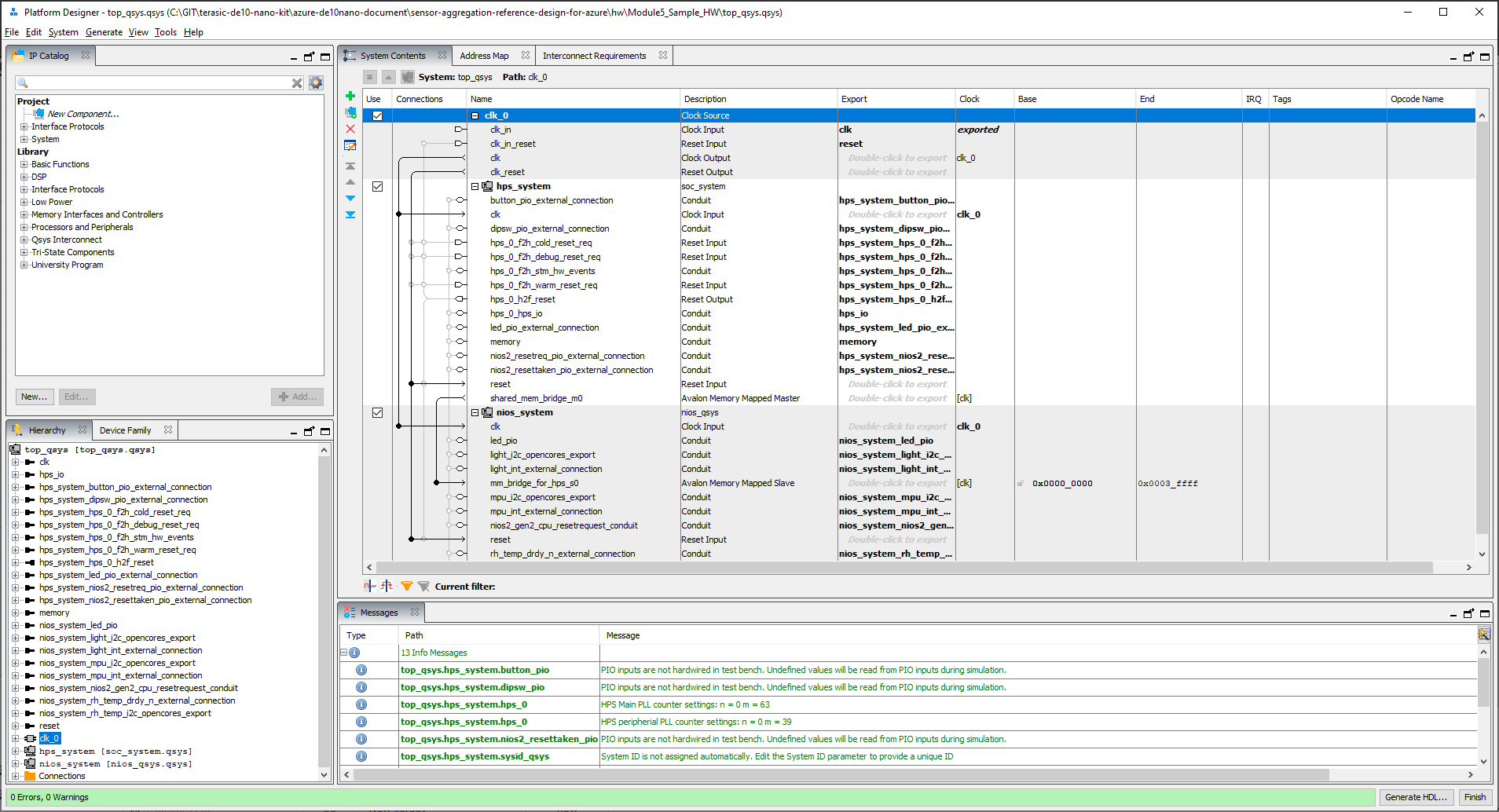
Figure 8: Top level of the QSYS design (Source Mouser)
To be able to modify the HPS system, we need to select the HPS system module and then drill down into the HPS System.
This will open the HPS design such that it shows the lower-level elements, including the HPS subsystem. Double click on the HPS system such that we can change the SPI from being connected to the HPS to being connected to the FPGA (Figure 9).
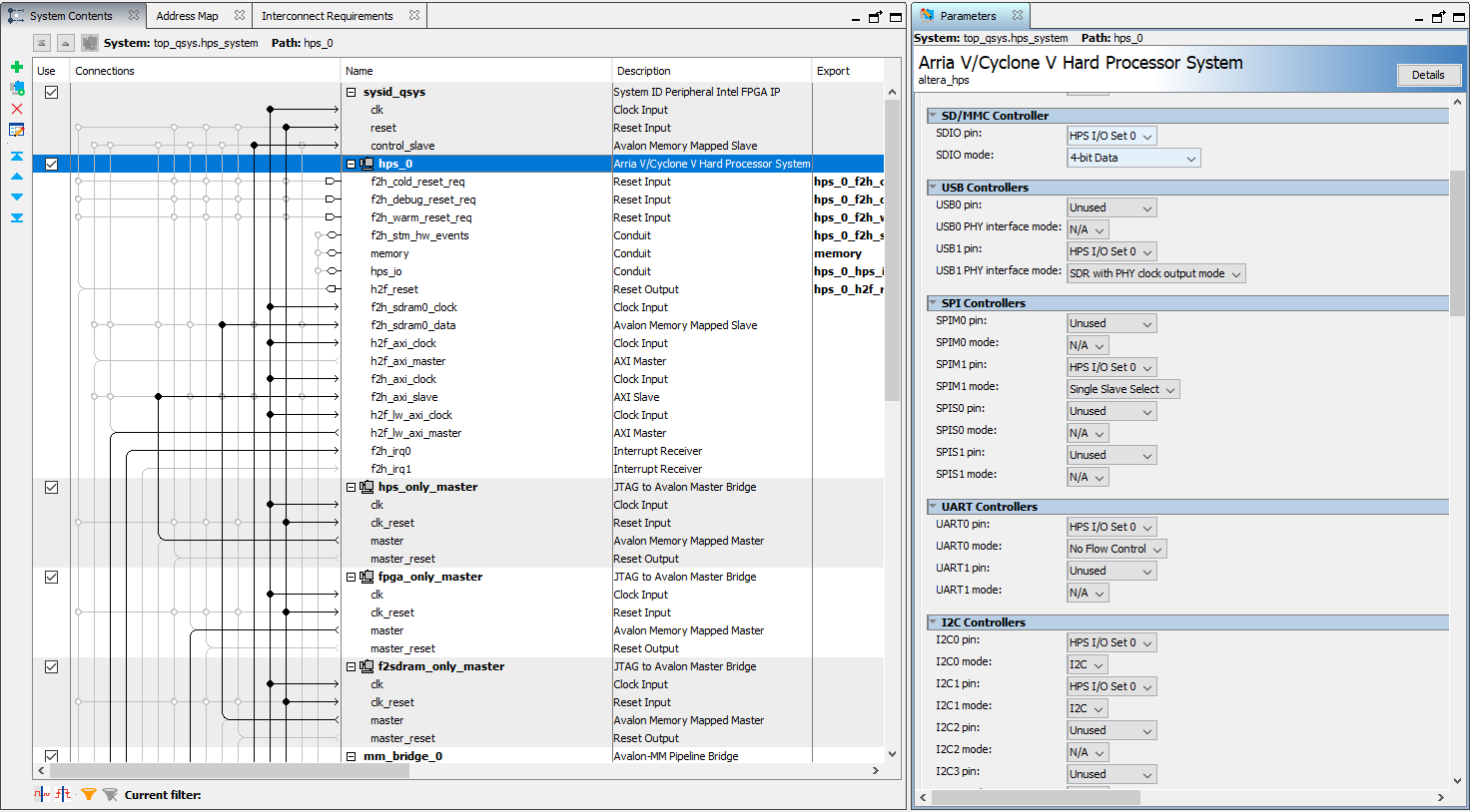
Figure 9: Customising the HPS (Source Mouser)
Once the SPIM1 has been set to the FPGA Fabric, we need to export the IO to the higher level; at the higher level, this output also need to be exported, making them available in the FPGA fabric.
In Platform Designer, if you want to see the breakout of the pins, you can view the block diagram (Figure 10), which should show the new SPI inputs and outputs.
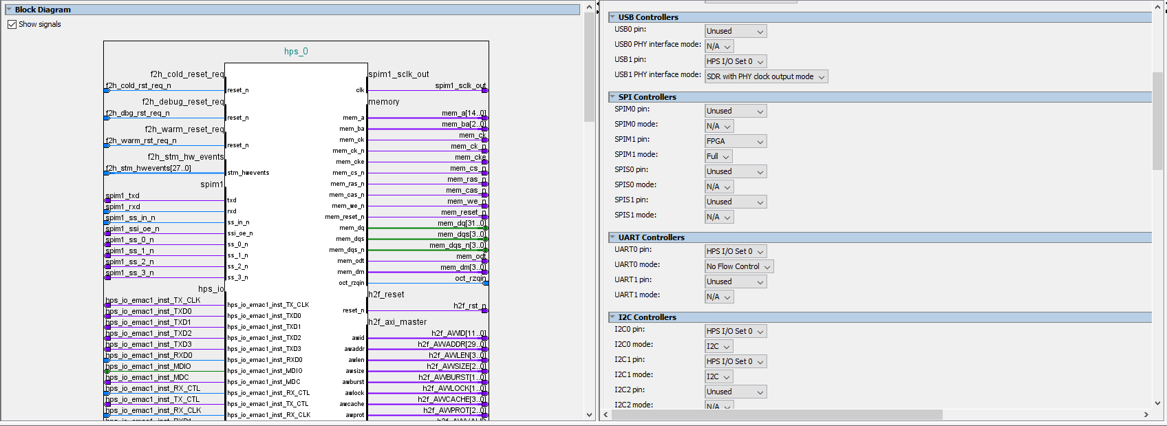
Figure 10: Block diagram showing the new pins (Source Mouser)
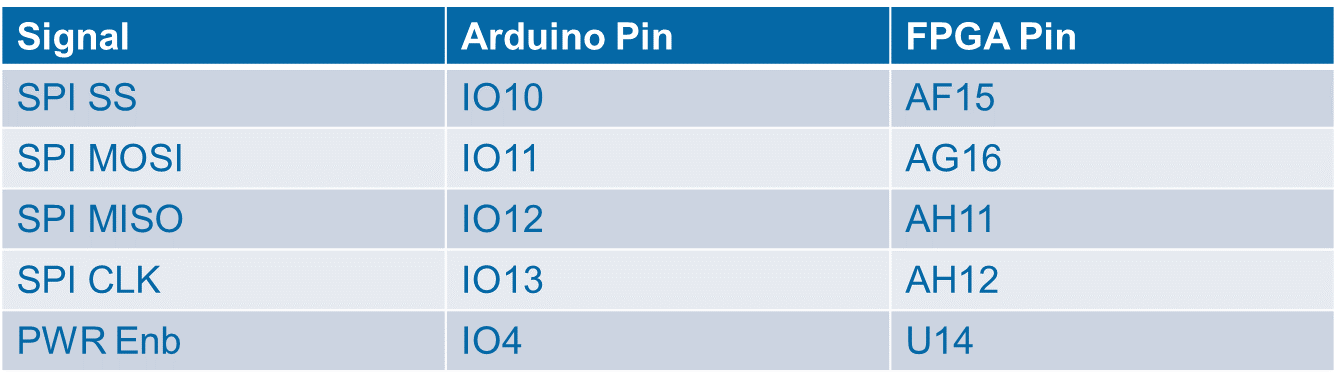
The next step in the design process is to update the top-level Verilog file to map in the new SPI IO. The allocation is shown in Table 1.
Table 1: SPI IO Allocations (Source Mouser Electronics)
To make these connections, we can use the pin planner in Quartus All the IO added should be set for LVCMOS3V3 Standard. This is shown in Figure 11.
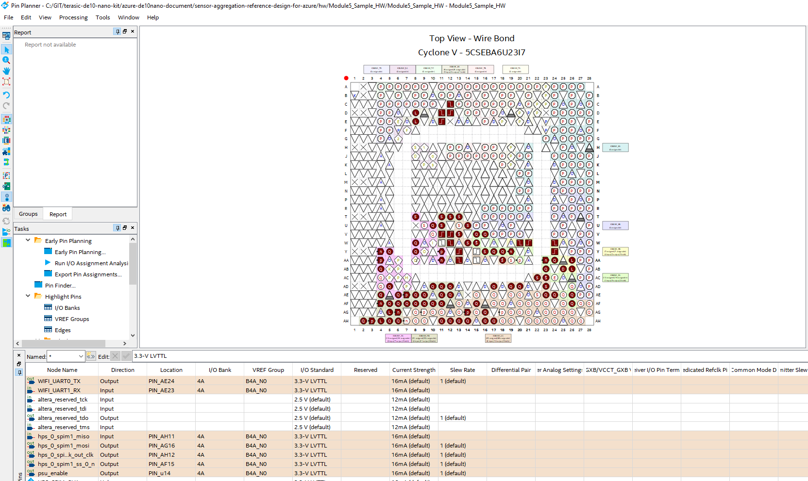
Figure 11: Additional pin allocation (Source Mouser)
Once this has been completed, we can then compile the design and generate the programming file as outlined in Figure 12.
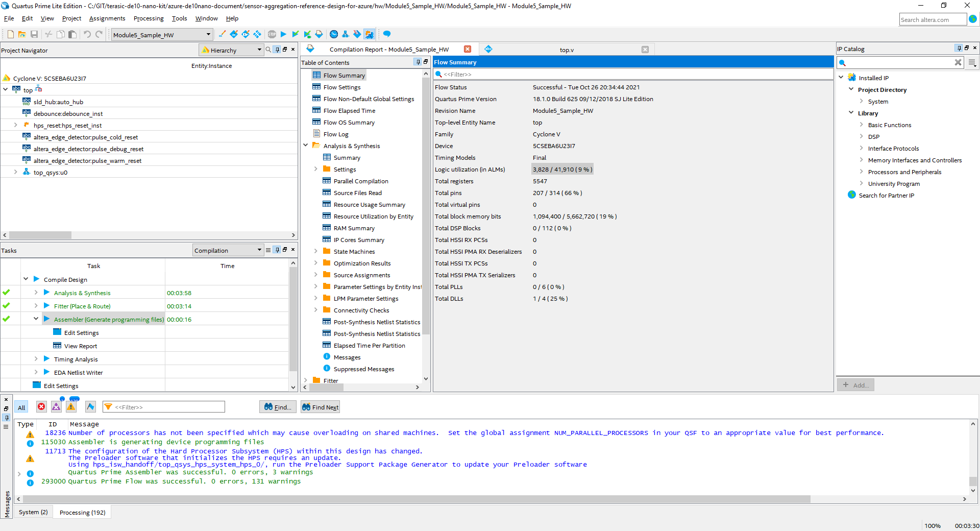
Figure 12: Building the project (Source Mouser)
To be able to change the FPGA Fabric design at run time in the FPGA, however, we need an RBF file and not the SOF generated in the compilation process.
As part of the example project, there is a sof_to_rbf.bat file located under the directory /Module5_Sample_HW/Output files. Double click on this bat file, and the RBF file will be created (Figure 13).
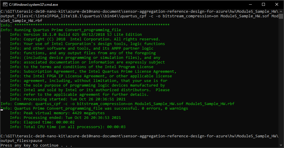
Figure 13: Additional pin allocation (Source Mouser)
Device Tree Overlay
Once this is completed, we also need to update and create a device tree overlay which describes the new elements of hardware added and any new bindings required for the example.
A device tree binding is providing under the directory <download directory>\terasic-de10-nano-kit\azure-de10nano-document\sensor-aggregation-reference-design-for-azure\hw\dtb
Examining this, you will see that it is a text file which describes the new nodes to the embedded Linux solution running on the HPS. This file also describes which of the RBF files is associated with the device tree and should be loaded into the FPGA Fabric when called.
/dts-v1/;
    /plugin/;
    /{
        fragment@0{
            target-path=”/soc/base-fpga-region”;
            #address-cells=<0x1>;
            #size-cells=<0x1>;
            __overlay__{
                #address-cells=<2>;
                #size-cells=<1>;
                //external-fpga-config;
                firmware-name=”Module5_Sample_HW.rbf”;
                fpga-bridges=<@fpga_bridge0&fpga_bridge1>;
                ranges=<0x00000000 0x00000000 0xc0000000 0x20000000>,
                    <0x00000001 0x00000000 0xff200000 0x00200000>;
            };
        };
    };
Into this device tree we need to add in device tree bindings for the IIO driver and the ADC7124. Once these have been added in, we are able to compile the device tree using SoCEDS embedded command shell, which includes the device tree compiler tool (Figure 14).
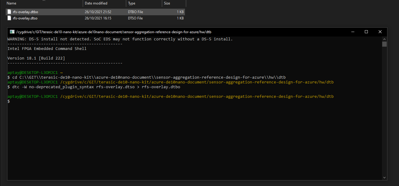
Figure 14: Compiling the DTSO (Source Mouser)
Uploading the Overlay
With both the overlay available and the Device Tree compiled, we can connect to the running DE10 Nano board and upload the dtbo and the rbf files generated to the /lib/firmware directory on the de10 nano. To do this, you can use either a command line SCP command or an application line WinSCP. The latter is what was used for this demonstration (Figure 15).
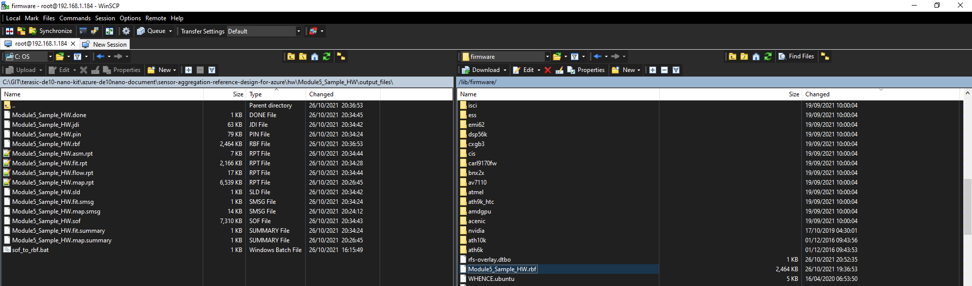
Figure 15: Uploading the overlays (Source Mouser)
Once the overlay has been uploaded, the next step is to run the overlay on the de10 nano. The first stage in this is to stop the overlay currently running.
We can do this by issuing the following commands in a de10 nano terminal:
systemctl stop lightdm
        echo 0>/sys/class/graphics/fbcon/cursor_blink
        rmdir /sys/kernel/config/device-tree/overlays/socfpga
        mkdir /sys/kernel/config/device-tree/overlays/socfpga
        echo rfs-overlay.dtbo >/sys/kernel/config/device-tree/overlays/socfpga/path
When the currently running overlay is stopped and removed, you should see the LED on top of the AD shield go out as the PSU enable is no longer supplied. As we load in the new overlay you should see light again as the PSU is re-enabled.
Now we have an overlay which is communicating with the sensor, and we can start development of the cloud application which will make use of the sensor in this overlay. Click the following link to continue with part two of this two-part series Terasic FPGA Cloud Connectivity Kit: Part Two (mouser.com)