MOSFET FAQs: 10 Essential Questions Answered

Image Source: ALEKSFILM/stock.adobe.com
By Simon Duggleby, Mouser
Published November 20, 2026
The sudden, unmistakable pop of a failing power device is a sound familiar to any engineer. More often than not, that acoustic failure indicates that a power semiconductor has been pushed past its limits by electrical, thermal, or transient overstress.
Although the world of power electronics is changing, silicon-based MOSFETs remain the most common type. To clear up common ambiguities in terminology, type, structure, usage, and selection, this guide focuses on silicon MOSFETs and answers 10 essential questions to help engineers with this mainstay electronic component.
What Does MOSFET Stand For?
MOSFET is an acronym for metal-oxide-semiconductor field-effect transistor. Each part of the name describes an aspect of its construction or operation:
- Metal: The gate electrode of the MOS structure. Although modern devices do not always use a metallic gate material, the original terminology has been retained.
- Oxide: The gate insulator layer, traditionally silicon dioxide.
- Semiconductor: The silicon substrate forming the conductive channel.
- Field effect: The voltage-driven control mechanism modulating conductivity via an electric field.
- Transistor: A semiconductor device that controls current or voltage and can be used for switching or amplification.
What Is a MOSFET?
A MOSFET is a voltage-controlled semiconductor used to switch or amplify signals. Unlike bipolar junction transistors (BJTs), MOSFETs do not require continuous control current during conduction, although their gates require transient current during switching.
While structurally a four-terminal device, the body is usually tied to the source, creating three terminals (Figures 1 and 2):
- Gate (G): The isolated control terminal that establishes the internal electric field.
- Drain (D): One of the two main current-carrying terminals. In conventional first-quadrant operation of an N-channel MOSFET, conventional current enters the drain and leaves the source, although an enhanced channel can conduct in either direction.
- Source (S): The reference terminal for gate-source voltage (VGS) and one of the main current-carrying terminals.
An insulating dielectric layer separates the gate from the channel, providing high input impedance by blocking DC conduction. This allows a gate voltage to efficiently control the current between source and drain.
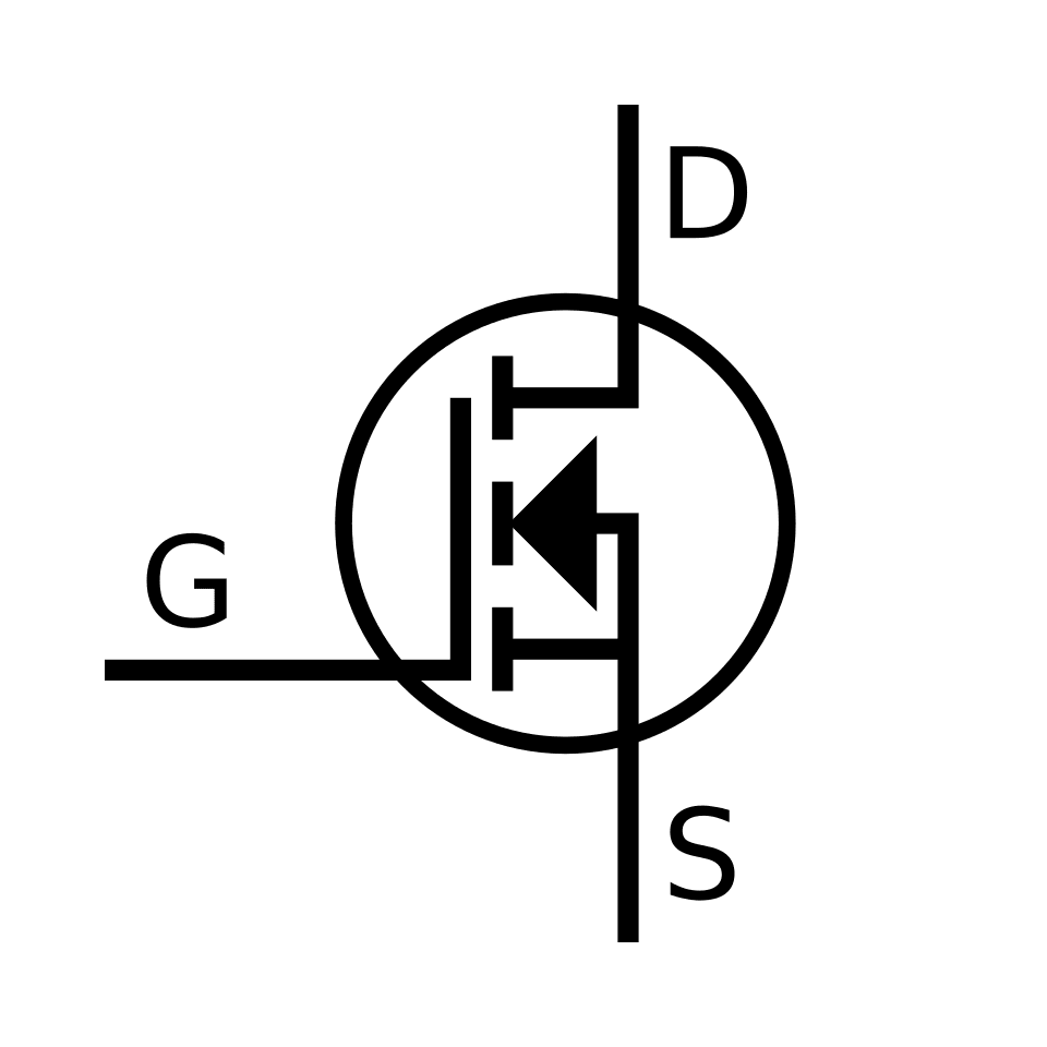
Figure 1: The schematic symbol for an N-channel MOSFET, with the gate, drain, and source labelled.
(Source: Public Domain, https://commons.wikimedia.org/w/index.php?curid=829685)
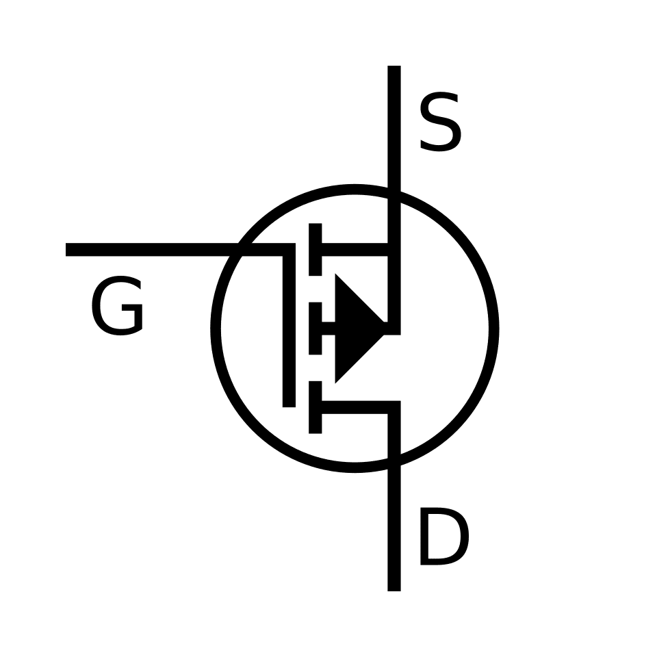
Figure 2: The schematic symbol for a P-channel MOSFET, with the gate, source, and drain labelled.
(Source: Public Domain, https://en.wikipedia.org/wiki/MOSFET#/media/File:IGFET_P-Ch_Enh_Labelled.svg)
How Does a MOSFET Differ from Other Transistors?
The MOSFET is a type of field-effect transistor (FET) that uses an insulated gate to control current flow between the drain and source terminals. The following are some of the key differences between MOSFETs and BJTs:
- Control parameter: Silicon MOSFETs are voltage-controlled devices that rely on the gate-source voltage (VGS), whereas BJTs are controlled by the base current (IB).
- Input impedance: Silicon MOSFETs have extremely high input impedance because the gate is insulated from the channel, while BJTs typically exhibit much lower input impedance.
- Drive requirements: MOSFETs require very little steady-state gate current, simplifying the design of gate-drive circuits. BJTs require a continuous base current while conducting.
- Switching speeds: MOSFETs generally switch faster than comparable power BJTs, making them well-suited for switching power supplies, motor drives, and other high-frequency applications.
- Temperature coefficient: When fully enhanced in the ohmic region, silicon power MOSFETs generally exhibit a positive temperature coefficient of RDS(on), which can improve static current sharing between properly matched and thermally coupled parallel devices.
These characteristics have made MOSFETs widely used in high-frequency switching and power-conversion applications, particularly at low and moderate voltage levels. Higher switching frequencies also enable the use of smaller magnetic components, helping create more compact and efficient systems.
What Is a MOSFET Used For?
MOSFETs are widely used for power switching, load control, signal amplification, and digital logic. Most applications can be grouped into four key areas:
- Power switching: The dominant switching device in DC-DC converters, switched-mode power supplies, inverters, and motor drives.
- Signal amplification: Used in many audio amplifiers, Radio frequency (RF) power stages, analogue integrated circuits, and active-load configurations.
- Logic circuits: Paired as complementary N-channel and P-channel devices to form energy-efficient Complementary metal-oxide-semiconductor (CMOS) logic used throughout modern digital electronics.
- Power distribution and load switching: Used as solid-state switches in battery management systems, eFuses, power-path control, hot-swap protection, and general load switching.
Explore more MOSFET use cases from a practical motor drive perspective in the Basics of MOSFETs and IGBTs for Motor Control application analysis.
How Does a MOSFET Work?
A MOSFET is controlled by the gate-to-source voltage (VGS), which determines whether current can flow between the drain and source. In an enhancement-mode MOSFET, the device is normally off, meaning little or no current flows when VGS is zero.
When a positive voltage is applied to the gate of an N-channel MOSFET, an electric field is created across the insulating oxide layer. This field attracts electrons toward the semiconductor surface beneath the gate, eventually creating a conductive channel. Once the gate voltage exceeds the threshold voltage (VTH), current can flow through this channel from the drain to the source.
Increasing the gate voltage strengthens this channel, reducing the device’s on-resistance (RDS(on)) and allowing it to conduct more efficiently.
What Are the Main Types of MOSFETs?
MOSFETs are commonly classified by their channel type (N-channel or P-channel) and operating mode (enhancement or depletion). Combining these characteristics produces four fundamental MOSFET variants:
- N-channel enhancement mode: The most common type used in power electronics. It is a normally OFF device that requires a positive VGS for conduction. Because electrons have higher mobility than holes in silicon, N-channel devices typically offer lower RDS (on), higher current capability, and better overall efficiency than equivalent P-channel devices.
- P-channel enhancement mode: A normally OFF device requiring a negative VGS to conduct. These are often used in high-side switching applications because they simplify gate-drive circuitry for positive supply rails.
- N-channel depletion mode: A normally ON device with a pre-existing channel. A current-conducting channel exists at VGS = 0V, so a negative VGS is required to deplete the channel and turn the device OFF. These devices are typically used in specialised applications, such as constant-current circuits, startup circuits, and fail-safe designs.
- P-channel depletion mode: A normally ON device requiring a positive VGS to turn OFF. This is the least common MOSFET variant, typically found in specialised analogue and process-specific applications.
For a deeper look into selecting these specific types, see the Ultimate Guide to Silicon MOSFET Technology.
What Is the Structure of a MOSFET?
The physical construction of an N-channel enhancement-mode MOSFET is built on a P-type silicon substrate. Two heavily doped N+ regions are formed in the substrate to serve as the source and drain. Above the area between them sits a thin layer of insulating silicon dioxide (SiO₂), topped by the gate electrode (Figure 3). The oxide layer insulates the gate from the underlying silicon, which gives rise to the device’s high input impedance.
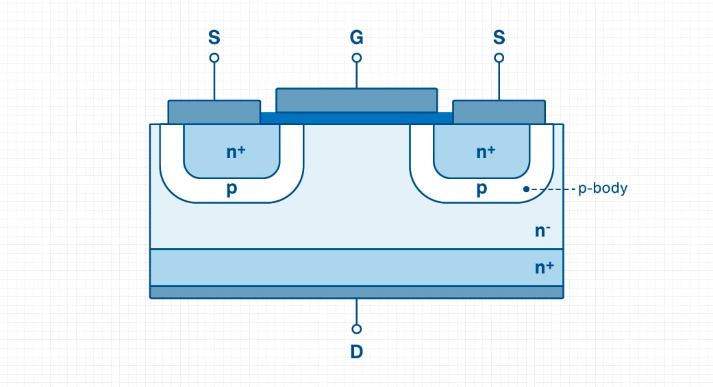
Figure 3: A cross-sectional diagram showing the internal structure of a MOSFET, highlighting the N-type and P-type materials, the oxide layer, and metal contacts. (Source: Mouser)
MOSFETs are available in three main structure types:
- Planar: These use a channel formed near the silicon surface. In power MOSFETs, current flows through a surface channel before passing vertically through the device to the drain.
- Trench: Vertical trenches contain the gate electrode and gate dielectric, forming channels along the trench sidewalls. This arrangement can increase cell density and reduce on-resistance, particularly in low- and medium-voltage power MOSFETs.
- Superjunction: This structure uses alternating columns of P-type and N-type material to improve the trade-off between breakdown voltage and on-resistance, enabling lower conduction losses at higher voltages.
How Do You Test a MOSFET on a Circuit Board?
When testing a MOSFET, initial diagnostics can be performed in-circuit, but definitive testing often requires removing the device.
The following steps present a typical troubleshooting process:
- Power down: Disconnect power and discharge all capacitors before making resistance or diode measurements.
- Check for shorts: With the gate discharged and held at the source potential, use a multimeter to check for an unintended low-resistance drain-to-source path. Use diode-test mode to check for the expected intrinsic body-diode conduction in the polarity appropriate to the device. These checks can identify gross failures but do not validate all MOSFET characteristics.
- Verify circuit operation: If energized testing can be performed safely, use appropriately rated differential or isolated measurement equipment to inspect the gate-to-source and drain-to-source waveforms. Do not connect an earth-referenced oscilloscope probe to a switching node unless the measurement arrangement is specifically designed for it.
- Remove and test, if necessary: If measurements prove inconclusive, remove the MOSFET from the PCB and test it separately. This eliminates the influence of surrounding components and provides a more reliable assessment of device health.
How Do You Use a MOSFET in a Circuit?
The exact implementation depends on the application, but most MOSFET switching circuits require attention to gate drive, load protection, thermal management, and PCB layout. Common design considerations include:
- Gate-drive voltage: Ensure the available gate-drive voltage is sufficient to fully enhance the MOSFET. The threshold voltage (VTH) indicates when conduction begins, not when the device reaches its specified low RDS(on).
- Gate resistor selection: A series resistor placed close to the gate pin helps control gate charging and discharging currents, manage switching speed, and reduce ringing and parasitic oscillation.
- Gate-to-source bias resistor: A resistor between the gate and source pins returns VGS to the device’s off-state value when the driver is inactive or in high-impedance mode. This is commonly called a pull-down resistor for a ground-referenced N-channel MOSFET.
- Flyback diode placement: When switching inductive loads such as relays, solenoids, or motors, a flyback diode is placed across the load to suppress potentially damaging voltage spikes during turn-off.
- Heat dissipation considerations: Conduction and switching losses generate heat within the MOSFET. Calculating these losses helps determine whether a heatsink or additional cooling is required.
- Layout optimisation: Minimising the inductance of gate and power loops helps reduce voltage overshoot, ringing, electromagnetic interference (EMI), and potential device stress.
What MOSFET Should I Buy?
MOSFET selection typically involves these key application-level requirements:
- Voltage rating: Choose a VDS rating comfortably above the highest operating and transient voltages.
- Current and conduction losses: Use the expected load current and RDS(on) to estimate conduction losses and temperature rise.
- Gate-drive compatibility: Ensure the available gate voltage is sufficient to fully enhance the MOSFET.
- Switching performance: For high-frequency applications, evaluate parameters such as gate charge (Qg) and output capacitance.
- Package and thermal management: Verify that the package and cooling arrangement can safely dissipate the expected power loss.
- Device technology: Trench MOSFETs generally dominate lower-voltage applications, while superjunction devices are widely used at higher voltages.
For a more in-depth guide on device selection, see the Ultimate Guide to Silicon MOSFET Technology, which offers a step-by-step process for selecting a silicon MOSFET.
Knowing When to Choose MOSFET Alternatives
While silicon MOSFETs are often a great choice for many applications, some alternatives can offer significant advantages under specific operating conditions:
- IGBTs: Often preferred in very high-power and high-voltage applications where switching frequencies are relatively low, such as wind turbines and large industrial motor drives.
- Silicon carbide (SiC) MOSFETs: Preferred for high-efficiency, high-temperature, and high-voltage power conversion. Currently popular for electric vehicle (EV) traction systems and high-power EV chargers.
- Gallium nitride (GaN) FETs: Ideal for ultra-high switching frequencies and high-power-density designs. Found in compact USB Type-C smartphone chargers and laptop power supplies.
For a detailed comparative breakdown for your technology selection, see Mouser’s guide on MOSFETs versus IGBTs. To source components for an active design, explore Mouser’s full inventory of MOSFETs.